- 制造厂商:TI
- 产品类别:接口
- 技术类目:其他接口
- 功能描述:SCSI 差动转换器 - 数据
- 点击这里打开及下载SN75971B的技术文档资料
- TI代理渠道,提供当日发货、严格的质量标准,满足您的目标价格

The SN75971B SCSI differential converter-data is a 9-channel RS-485 transceiver. When used in conjunction with its companion control transceiver, the SN75970B, the resulting chip set provides the superior electrical performance of differential SCSI from a single-ended SCSI bus or controller. A 16-bit Ultra-SCSI (or Fast-20) SCSI bus can be implemented with just three devices (two data and one control) in the space efficient, 56-pin, shrink small-outline package (SSOP) or thin shink small outline package (TSSOP) and a few external components. An 8-bit SCSI bus requires only one data and one control transceiver.
The SN75971B is available in a B2 (20 Mxfer) version and a B1 (10 Mxfer) version.
In a typical differential SCSI node, the SCSI controller provides an enable for each external RS-485 transceiver channel. This could require as many as 27
extra terminals for a 16-bit differential bus controller or relegate a 16-bit, single-ended controller to only an 8-bit differential bus. Using the standard nine SCSIcontrol signals, the SN75970B control transceiver decodes the state of the bus and enables the SN75971B data transceiver to transmit the single-ended SCSI input signals (A side) differentially to the cable or receive the differential cable signals (B side) and drive the single-ended outputs to the controller.
A reset function, which disables all outputs and clears internal latches, can be accomplished from two external inputs and two internally-generated signals. RESET\ (reset) and DSENS (differential sense) are available to external circuits for a bus reset or to disable all outputs should a single-ended cable be inadvertently connected to a differential connector. Internally-generated power-up and thermal-shutdown signals have the same affect when the supply voltage is below approximately 3.5 V or the junction temperature exceeds 175°C.
The SCSI, differential, converter-data chip operates in two modes depending on the state of the DRVBUS input. With DRVBUS low, a bidirectional latch circuit sets the direction of data transfer. Each data bit has its own latch, and each bit's direction is independent of all other bits. When neither the single-ended nor the differential sides are asserted, the latch disables both A- and B-side output drivers. When the input to either side is asserted, the latch enables the opposite side's driver and sets data flow from the asserted input to the opposite side of the device. When the input deasserts, the latch maintains the direction until the receiver on the enabled driver detects a deassertion. The latch then returns to the initial state. No parity checking is done by this device; the parity signal passes through the device like other data signals do.
When DRVBUS is high, direction is determined by the SDB signal. However, a change in SDB does not always immediately change the direction. When DRVBUS first asserts, the direction indicated by SDB is latched and takes effect immediately. When SDB changes while DRVBUS is high, the drivers that were on immediately turn off. However, the other driver set does not turn on until the receivers sense a deasserted state on all nine data lines. This is done to prevent the active drivers from turning on until all other drivers are off and the terminators pull the lines to a deasserted state.
The single-ended SCSI bus interface consists of CMOS, bidirectional inputs and outputs. The drivers are rated to ±16 mA of output current. The receiver inputs are pulled high with approximately 4 mA to eliminate the need for external pullup resistors for the open-drain outputs of most single-ended SCSI controllers. The single-ended side of the device is not intended to drive the SCSI bus directly.
The differential SCSI bus interface consists of bipolar, bidirectional inputs and outputs that meet or exceed the requirements of EIA-485 and ISO 8482-1982/TIA TR30.2 referenced by American National Standard of Information Systems (ANSI) X3.131-1994 Small Computer System Interface-2 (SCSI-2) and SCSI-3 Fast-20 Parallel Interface (Fast-20) X3.277:1996.
The SN75971B is characterized for operation over the temperature range of 0°C to 70°C.
- Provides High-Voltage Differential SCSI From Single-Ended Controller When Used With the SN75970B Control Transceiver
- Meets or Exceeds the Requirements of EIA Standard RS-485 and ISO-8482 Standards
- ESD Protection on Bus Pins to 12 kV
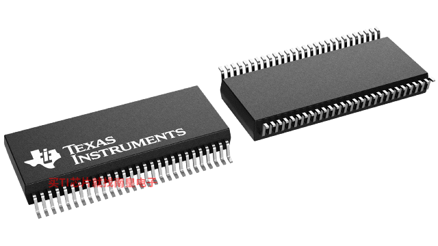
- Packaged in Shrink Small-Outline Package with 25 mil Terminal Pitch and Thin Small-Package with 20 mil Terminal Pitch
- Low Disabled-Supply Current 32 mA Typ
- Thermal Shutdown Protection
- Positive- and Negative-Current Limiting
- Power-Up/-Down Glitch Protection
- Open-Circuit Failsafe Receivers
- Operating temperature range (C)
- 0 to 70
SN75971B的完整型号有:SN75971B2DL,以下是这些产品的关键参数及官网采购报价:
SN75971B2DL,工作温度:0 to 70,封装:SSOP (DL)-56,包装数量MPQ:20个,MSL 等级/回流焊峰值温度:Level-2-260C-1 YEAR,引脚镀层/焊球材料:NIPDAU,TI官网SN75971B2DL的批量USD价格:17.08(1000+)

PSPICE-FOR-TI ― 适用于 TI 设计和模拟工具的 PSpice
PSpice for TI 可提供帮助评估模拟电路功能的设计和仿真环境。此功能齐全的设计和仿真套件使用 Cadence 的模拟分析引擎。PSpice for TI 可免费使用,包括业内超大的模型库之一,涵盖我们的模拟和电源产品系列以及精选的模拟行为模型。借助?PSpice for TI 的设计和仿真环境及其内置的模型库,您可对复杂的混合信号设计进行仿真。创建完整的终端设备设计和原型解决方案,然后再进行布局和制造,可缩短产品上市时间并降低开发成本。
在?PSpice for TI 设计和仿真工具中,您可以搜索 TI (...)
TINA-TI ― 基于 SPICE 的模拟仿真程序
TINA-TI 提供了 SPICE 所有的传统直流、瞬态和频域分析以及更多。TINA 具有广泛的后处理功能,允许您按照希望的方式设置结果的格式。虚拟仪器允许您选择输入波形、探针电路节点电压和波形。TINA 的原理图捕获非常直观 - 真正的“快速入门”。TINA-TI 安装需要大约 500MB。直接安装,如果想卸载也很容易。我们相信您肯定会爱不释手。
TINA 是德州仪器 (TI) 专有的 DesignSoft 产品。该免费版本具有完整的功能,但不支持完整版 TINA 所提供的某些其他功能。
如需获取可用 TINA-TI 模型的完整列表,请参阅:SpiceRack - 完整列表
需要 HSpice (...)