- 制造厂商:TI
- 产品类别:接口
- 技术类目:LVDS、M-LVDS 和 PECL IC
- 功能描述:5V 双路全双工 PECL 收发器
- 点击这里打开及下载TB5T1的技术文档资料
- TI代理渠道,提供当日发货、严格的质量标准,满足您的目标价格

The TB5T1 device is a dual differential driver/receiver circuit that transmits and receives digital data over balanced transmission lines. The dual drivers translate input TTL logic levels to differential pseudo-ECL output levels. The dual receivers convert differential-input logic levels to TTL output levels. Each driver or receiver pair has its own common enable control allowing serial data and a control clock to be transmitted and received on a single integrated circuit. The TB5T1 requires the customer to supply termination resistors on the circuit board.
The power-down loading characteristics of the receiver input circuit are approximately 8 k relative to the power supplies; hence, it does not load the transmission line when the circuit is powered down.
In circuits with termination resistors, the line remains impedance- matched when the circuit is powered down. The driver does not load the line when it is powered down.
All devices are characterized for operation from -40°C to 85°C.
The logic inputs of this device include internal pull-up resistors of approximately 40 k that are connected to VCC to ensure a logical high level input if the inputs are open circuited.
- Functional Replacement for the Agere BTF1A
- Driver Features
- Third-State Logic Low Output
- ESD Protection HBM > 3 kV, CDM > 2 kV
- No Line Loading when VCC = 0
- Capable of Driving 50- loads
- 2.0-ns Maximum Propagation Delay
- 0.2-ns Output Skew (typical)
- Receiver Features
- High-Input Impedance Approximately 8 k
- 4.0-ns Maximum Propagation Delay
- 50-mV Hysteresis
- Slew Rate Limited (1 ns min 80% to 20%)
- ESD Protection HBM > 3 kV, CDM > 2 kV
- -1.1-V to 7.1-V Input Voltage Range
- Common Device Features
- Common Enable for Each Driver/Receiver Pair
- Operating Temperature Range: -40°C to 85°C
- Single 5.0 V ± 10% Supply
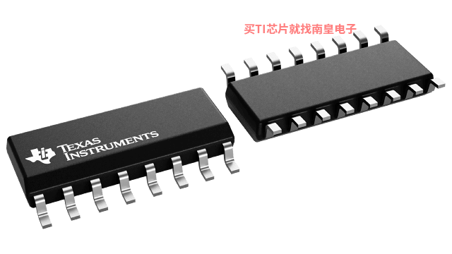
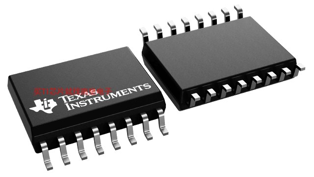
- Available in Gull-Wing SOIC (JEDEC MS-013, DW) and SOIC (D) Package
- Function
- Transceiver
- Protocols
- PECL
- Number of transmitters
- 2
- Number of receivers
- 2
- Supply voltage (V)
- 5
- Signaling rate (Mbps)
- 100
- Input signal
- PECL, TTL
- Output signal
- PECL, TTL
- Rating
- Catalog
- Operating temperature range (C)
- -40 to 85
TB5T1的完整型号有:TB5T1D、TB5T1DW、TB5T1DWR,以下是这些产品的关键参数及官网采购报价:
TB5T1D,工作温度:-40 to 85,封装:SOIC (D)-16,包装数量MPQ:40个,MSL 等级/回流焊峰值温度:Level-2-250C-1YEAR/Level-1-220C-UNLIM,引脚镀层/焊球材料:NIPDAU,TI官网TB5T1D的批量USD价格:8.289(1000+)
TB5T1DW,工作温度:-40 to 85,封装:SOIC (DW)-16,包装数量MPQ:40个,MSL 等级/回流焊峰值温度:Level-2-260C-1 YEAR,引脚镀层/焊球材料:NIPDAU,TI官网TB5T1DW的批量USD价格:9.796(1000+)
TB5T1DWR,工作温度:-40 to 85,封装:SOIC (DW)-16,包装数量MPQ:2000个,MSL 等级/回流焊峰值温度:Level-2-250C-1YEAR/Level-1-220C-UNLIM,引脚镀层/焊球材料:NIPDAU,TI官网TB5T1DWR的批量USD价格:8.665(1000+)

TB5T1DW IBIS Model
PSpice for TI 可提供帮助评估模拟电路功能的设计和仿真环境。此功能齐全的设计和仿真套件使用 Cadence 的模拟分析引擎。PSpice for TI 可免费使用,包括业内超大的模型库之一,涵盖我们的模拟和电源产品系列以及精选的模拟行为模型。借助?PSpice for TI 的设计和仿真环境及其内置的模型库,您可对复杂的混合信号设计进行仿真。创建完整的终端设备设计和原型解决方案,然后再进行布局和制造,可缩短产品上市时间并降低开发成本。
在?PSpice for TI 设计和仿真工具中,您可以搜索 TI (...)
TINA-TI ― 基于 SPICE 的模拟仿真程序
TINA-TI 提供了 SPICE 所有的传统直流、瞬态和频域分析以及更多。TINA 具有广泛的后处理功能,允许您按照希望的方式设置结果的格式。虚拟仪器允许您选择输入波形、探针电路节点电压和波形。TINA 的原理图捕获非常直观 - 真正的“快速入门”。TINA-TI 安装需要大约 500MB。直接安装,如果想卸载也很容易。我们相信您肯定会爱不释手。
TINA 是德州仪器 (TI) 专有的 DesignSoft 产品。该免费版本具有完整的功能,但不支持完整版 TINA 所提供的某些其他功能。
如需获取可用 TINA-TI 模型的完整列表,请参阅:SpiceRack - 完整列表
需要 HSpice (...)


