- ���쳧�̣�TI
- ��Ʒ�������ת����
- ������Ŀ��ģ��ת���� (ADC) - ����ģ��ת���� (<=10MSPS)
- ����������12 λ��������������ģ���������ת��ʱ�Ӻ� 8x FIFO��4 ͨ��
- ������������TLC2574�ļ����ĵ�����
- TI�����������ṩ���շ������ϸ������������������Ŀ��۸�

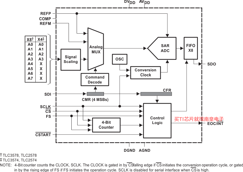
The TLC3574, TLC3578, TLC2574, and TLC2578 are a family of high-performance, low-power, CMOS analog-to-digital converters (ADC). TLC3574/78 is a 14-bit ADC; TLC2574/78 is a 12-bit ADC. All parts operate from single 5-V analog power supply and 3-V to 5-V digital supply. The serial interface consists of four digital input [chip select (CS\), frame sync (FS), serial input-output clock (SCLK), serial data input (SDI)], and a 3-state serial data output (SDO). CS\ (works as SS\, slave select), SDI, SDO and SCLK form an SPI interface. FS, SDI, SDO, and SCLK form DSP interface. The frame sync signal (FS) indicates the start of a serial data frame being transferred. When multiple converters connect to one serial port of a DSP, CS\ works as the chip select to allow the host DSP to access the individual converter. CS\ can be tied to ground if only one converter is used. FS must be tied to DVDD if it is not used (such as in an SPI interface). When SDI is tied to DVDD, the device is set in hardware default mode after power on and no software configuration is required. In the simplest case, only three wires (SDO, SCLK, and CS\ or FS) are needed to interface with the host.
In addition to being a high-speed ADC with versatile control capability, these devices have an on-chip analog multiplexer (MUX) that can select any analog input or one of three self-test voltages. The sample-and-hold function is automatically started after the fourth SCLK (normal sampling) or can be controlled by a special pin, CSTART\, to extend the sampling period (extended sampling). The normal sampling period can also be programmed as short sampling (12 SCLKs) or long sampling (44 SCLKs) to accommodate the faster SCLK operation popular among high-performance signal processors. The TLC3574/78 and TLC2574/78 are designed to operate with low-power consumption. The power saving feature is further enhanced with autopower-down mode and programmable conversion speeds. The conversion clock (internal OSC) is built in. The converter can also use an external SCLK as the conversion clock for maximum flexibility. The TLC3574/78 and TLC2574/78 are specified with bipolar input and a full scale range of ±10 V.
- 14-Bit Resolution for TLC3574/78, 12-Bit for TLC2574/2578
- Maximum Throughput 200-KSPS
- Multiple Analog Inputs:
- 8 Single-Ended Channels for TLC3578/2578
- 4 Single-Ended Channels for TLC3574/2574
- Analog Input Range: ��10 V
- Pseudodifferential Analog Inputs
- SPI/DSP-Compatible Serial Interfaces With SCLK up to 25-MHz
- Built-In Conversion Clock and 8x FIFO
- Single 5-V Analog Supply; 3-/5-V Digital Supply
- Low-Power
- 5.8 mA in Normal Operation
- 20 ��A in Power Down
- Programmable Autochannel Sweep and Repeat
- Hardware-Controlled, Programmable Sampling Period
- Hardware Default Configuration
- INL: TLC3574/78: ��1 LSB; TLC2574/78: ��0.5 LSB
- DNL: TLC3574/78: ��0.5 LSB; TLC2574/78: ��0.5 LSB
- SINAD: TLC3574/78: 79 dB; TLC2574/78: 72 dB
- THD: TLC3574/78: �C82 dB; TLC2574/78: �C82 dB
Note: Recommended Voltage Reference: REF02 and REF102
- Resolution (Bits)
- 12
- Number of input channels
- 4
- Sample rate (Max) (kSPS)
- 200
- Interface type
- SPI
- Architecture
- SAR
- Input type
- Pseudo-Differential, Single-Ended
- Multi-channel configuration
- Multiplexed
- Rating
- Catalog
- Reference mode
- Ext
- Input range (Max) (V)
- 10
- Input range (Min) (V)
- -10
- Features
- Oscillator
- Operating temperature range (C)
- -40 to 85
- Power consumption (Typ) (mW)
- 29
- Analog voltage AVDD (Min) (V)
- 4.75
- SNR (dB)
- 72
- Analog voltage AVDD (Max) (V)
- 5.5
- INL (Max) (+/-LSB)
- 1
- Digital supply (Min) (V)
- 2.7
- Digital supply (Max) (V)
- 5.5
TLC2574�������ͺ��У�TLC2574IDW��TLC2574IPW����������Щ��Ʒ�Ĺؼ������������ɹ����ۣ�
TLC2574IDW�������¶ȣ�-40 to 85����װ��SOIC (DW)-20����װ����MPQ��25����MSL �ȼ�/��������ֵ�¶ȣ�Level-1-260C-UNLIM�����ŶƲ�/������ϣ�NIPDAU��TI����TLC2574IDW������USD�۸�7.403��1000+��
TLC2574IPW�������¶ȣ�-40 to 85����װ��TSSOP (PW)-20����װ����MPQ��70����MSL �ȼ�/��������ֵ�¶ȣ�Level-1-260C-UNLIM�����ŶƲ�/������ϣ�NIPDAU��TI����TLC2574IPW������USD�۸�7.403��1000+��

TLC2574 IBIS Model
PSpice for TI ���ṩ��������ģ���·���ܵ���ƺͷ��滷�����˹�����ȫ����ƺͷ�����ʹ�� Cadence ��ģ��������档PSpice for TI �����ʹ�ã�����ҵ�ڳ����ģ�Ϳ�֮һ���������ǵ�ģ��͵�Դ��Ʒϵ���Լ���ѡ��ģ����Ϊģ�͡�����?PSpice for TI ����ƺͷ��滷���������õ�ģ�Ϳ⣬���ɶԸ��ӵĻ���ź���ƽ��з��档�����������ն��豸��ƺ�ԭ�ͽ��������Ȼ���ٽ��в��ֺ����죬�����̲�Ʒ����ʱ�䲢���Ϳ����ɱ���
��?PSpice for TI ��ƺͷ��湤���У����������� TI (...)
TINA-TI �� ���� SPICE ��ģ��������
TINA-TI �ṩ�� SPICE ���еĴ�ͳֱ����˲̬��Ƶ������Լ����ࡣTINA ���й㷺�ĺ������ܣ�����������ϣ���ķ�ʽ���ý���ĸ�ʽ����������������ѡ�����벨�Ρ�̽���·�ڵ��ѹ�Ͳ��Ρ�TINA ��ԭ��ͼ����dz�ֱ�� - �����ġ��������š���TINA-TI ��װ��Ҫ��Լ 500MB��ֱ�Ӱ�װ�������ж��Ҳ�����ס������������϶��ᰮ�����֡�
TINA �ǵ������� (TI) ר�е� DesignSoft ��Ʒ������Ѱ汾���������Ĺ��ܣ�����֧�������� TINA ���ṩ��ijЩ�������ܡ�
�����ȡ���� TINA-TI ģ�͵������б�������ģ�SpiceRack - �����б�
��Ҫ HSpice (...)
ADC-INPUT-CALC �� Analog-to-digital converter (ADC) input driver design tool supporting multiple input types
ADC-INPUT-CALC ��һ�����߹��ߣ���Ϊ���ģ��ת���� (ADC) �����뻺�����ṩ֧�֡����ṩ 24 �ֲ�ͬ�Ļ�������Ŵ����Ļ�������·����Щ��·���������� ADC ���롣�������˺��Dz�ֵ��˺ͱ�ѹ�����������ơ�֧�ֽ�����Ϻ�ֱ���������Լ�����Դ��˫��Դ���ˡ��ṩ����ģʽ����ѧ��ģʽ��ר��ģʽ���ڳ�ѧ��ģʽ�У������Ա�Ȼش�һϵ�����⣬Ȼ��ῴ���������ԭ��ͼ����ijЩ����£����ῴ����������Ŀ�ѡ�汾����ר��ģʽ�£������Ա�ῴ���÷���ͼ��ʽ��ʾ������ 24 (...)ANALOG-ENGINEER-CALC �� ģ���ʦ������
ģ���ʦ������ּ�ڼӿ�ģ���·��ƹ���ʦ����ʹ�õ������ظ��Լ��㡣�û��� PC �Ĺ����ṩͼ�ν��棬������ʾ���ֳ���������б�����ʹ�÷�����������������Ŵ������浽Ϊ�ȶ�ģ��ת���� (ADC) ��������������·ѡ����ʵĵ�·���Ԫ���������˿����������Ĺ���֮�⣬�ü��������ܹ��ܺõ���ģ���ʦ�ڴ��ο����������ĸ������ʹ�á� lock = ��Ҫ�������ɣ�1���ӣ�