- 制造厂商:TI
- 产品类别:音频
- 技术类目:音频转换器 - 音频编解码器
- 功能描述:独立于采样速率的单通道编解码器带宽
- 点击这里打开及下载TLC320AC01的技术文档资料
- TI代理渠道,提供当日发货、严格的质量标准,满足您的目标价格

The TLC320AC01 analog interface circuit (AIC) is an audio-band processor that provides an analog-to-digital and digital-to-analog input/output interface system on a single monolithic CMOS chip. This device integrates a band-pass switched-capacitor antialiasing input filter, a 14-bit-resolution analog-to-digital converter (ADC), a 14-bit-resolution digital-to-analog converter (DAC), a low-pass switched-capacitor output-reconstruction filter, (sin x)/x compensation, and a serial port for data and control transfers.
The internal circuit configuration and performance parameters are determined by reading control information into the eight available data registers. The register data sets up the device for a given mode of operation and application.
The major functions of the TLC320AC01 are: 1. To convert audio-signal data to digital format by the ADC channel 2. To provide the interface and control logic to transfer data between its serial input and output terminals and a digital signal processor (DSP) or microprocessor 3. To convert received digital data back to an audio signal through the DAC channel
The antialiasing input low-pass filter is a switched-capacitor filter with a sixth-order elliptic characteristic. The high-pass filter is a single-pole filter to preserve low-frequency response as the low-pass filter cutoff is adjusted. There is a three-pole continuous-time filter that precedes this filter to eliminate any aliasing caused by the filter clock signal.
The output-reconstruction switched-capacitor filter is a sixth-order elliptic transitional low-pass filter followed by a second-order (sin x)/x correction filter. This filter is followed by a three-pole continuous-time filter to eliminate images of the filter clock signal.
The TLC320AC01 consists of two signal-processing channels, an ADC channel and a DAC channel, and the associated digital control. The two channels operate synchronously; data reception at the DAC channel and data transmission from the ADC channel occur during the same time interval. The data transfer is in2s-complement format.
There are three basic modes of operation available: the stand-alone analog-interface mode, the master-slave mode, and the linear-codec mode. In the stand-alone mode, the TLC320AC01 generates the shift clock and frame synchronization for the data transfers and is the only AIC used. The master-slave mode has one TLC320AC01 as the master that generates the master-shift clock and frame synchronization; the remaining AICs are slaves to these signals. In the linear-codec mode, the shift clock and the frame-synchronization signals are externally generated and the timing can be any of the standard codec-timing patterns.
Typical applications for this device include modems, speech processing, analog interface for DSPs, industrial-process control, acoustical-signal processing, spectral analysis, data acquisition, and instrumentation recorders.
The TLC320AC01C is characterized for operation from 0°C to 70°C.
- General-Purpose Signal-Processing Analog Front End (AFE)
- Single 5-V Power Supply
- Power Dissipation . . . 100 mW Typ
- Signal-to-Distortion Ratio . . . 70 dB Typ
- Programmable Filter Bandwidths (Up to 10.8 kHz) and Synchronous ADC and DAC Sampling
- Serial-Port Interface
- Monitor Output With Programmable Gains of 0 dB, \x968 dB, \x96 18 dB, and Squelch
- Two Sets of Differential Inputs With Programmable Gains of 0 dB, 6 dB, 12 dB, and Squelch
- Differential or Single-Ended Analog Output With Programmable Gains of 0 dB, \x966 dB, \x96 12 dB, and Squelch
- Differential Outputs Drive 3-V Peak Into a 600- Differential Load
- Differential Architecture Throughout
- 1-um Advanced LinEPICTM Process
- 14-Bit Dynamic-Range ADC and DAC
- 2s-Complement Data Format
- Application Report Available
The TLC320AC01 is functionally equivalent to the TLC320AC02 and differs in the electrical specifications as shown in Appendix C. Designing with the TLC320AC01 Analog Interface for DSPs (SLAA006) LinEPIC is a trademark of Texas Instruments Incorporated.
- Number of ADC channels
- 4
- Number of DAC channels (#)
- 1
- Analog inputs
- 2
- Sampling rate (Max) (kHz)
- 25
- Rating
- Military
- ADC SNR (Typ) (dB)
- 0
- DAC SNR (Typ) (dB)
- 0
TLC320AC01的完整型号有:TLC320AC01CFN、TLC320AC01CFNR、TLC320AC01CPM,以下是这些产品的关键参数及官网采购报价:
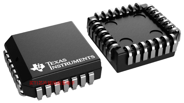
TLC320AC01CFN,工作温度:0 to 70,封装:PLCC (FN)-28,包装数量MPQ:37个,MSL 等级/回流焊峰值温度:Level-4-260C-72 HR,引脚镀层/焊球材料:NIPDAU,TI官网TLC320AC01CFN的批量USD价格:6.946(1000+)
TLC320AC01CFNR,工作温度:0 to 70,封装:PLCC (FN)-28,包装数量MPQ:750个,MSL 等级/回流焊峰值温度:Level-4-260C-72 HR,引脚镀层/焊球材料:NIPDAU,TI官网TLC320AC01CFNR的批量USD价格:5.788(1000+)
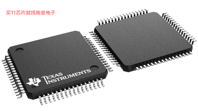
TLC320AC01CPM,工作温度:0 to 70,封装:LQFP (PM)-64,包装数量MPQ:160个,MSL 等级/回流焊峰值温度:Level-3-220C-168 HR,引脚镀层/焊球材料:NIPDAU,TI官网TLC320AC01CPM的批量USD价格:6.946(1000+)

PSPICE-FOR-TI ― 适用于 TI 设计和模拟工具的 PSpice
PSpice for TI 可提供帮助评估模拟电路功能的设计和仿真环境。此功能齐全的设计和仿真套件使用 Cadence 的模拟分析引擎。PSpice for TI 可免费使用,包括业内超大的模型库之一,涵盖我们的模拟和电源产品系列以及精选的模拟行为模型。借助?PSpice for TI 的设计和仿真环境及其内置的模型库,您可对复杂的混合信号设计进行仿真。创建完整的终端设备设计和原型解决方案,然后再进行布局和制造,可缩短产品上市时间并降低开发成本。
在?PSpice for TI 设计和仿真工具中,您可以搜索 TI (...)


