- ÷Τ‘λ≥ß…ΧΘΚTI
- ≤ζΤΖάύ±πΘΚΫ”ΩΎ
- ΦΦ θάύΡΩΘΚΤδΥϊΫ”ΩΎ
- ΙΠΡήΟη ωΘΚ0.6Gbps ÷Ν 1.5Gbps ’ΖΔΤς
- ΒψΜς’βάο¥ρΩΣΦΑœ¬‘ΊTLK1501ΒΡΦΦ θΈΡΒΒΉ Νœ
- TI¥ζάμ«ΰΒάΘ§ΧαΙ©Β±»’ΖΔΜθΓΔ―œΗώΒΡ÷ ΝΩ±ξΉΦΘ§¬ζΉψΡζΒΡΡΩ±ξΦέΗώ

The TLK1501 is a member of the transceiver family of multigigabit transceivers used in ultrahigh-speed bidirectional point-to-point data transmission systems. The TLK1501 supports an effective serial interface speed of 0.6 Gbps to 1.5 Gbps, providing up to 1.2 Gbps of data bandwidth. The TLK1501 is pin-for-pin compatible with the TLK2500. The TLK1501 is both pin-for-pin compatible with and functionally identical to the TLK2501, a 1.6 to 2.5 Gbps transceiver, and the TLK3101, a 2.5 to 3.125 Gbps transceiver, providing a wide range of performance solutions with no required board layout changes.
The primary application of this chip is to provide very high-speed I/O data channels for point-to-point baseband data transmission over controlled impedance media of approximately 50  . The transmission media can be printed-circuit board, copper cables, or fiber-optic cable. The maximum rate and distance of data transfer is dependent upon the attenuation characteristics of the media and the noise coupling to the environment.
This device can also be used to replace parallel data transmission architectures by providing a reduction in the number of traces, connector terminals, and transmit/receive terminals. Parallel data loaded into the transmitter is delivered to the receiver over a serial channel, which can be a coaxial copper cable, a controlled impedance backplane, or an optical link. It is then reconstructed into its original parallel format. It offers significant power and cost savings over current solutions, as well as scalability for higher data rate in the future.
The TLK1501 performs data conversion parallel-to-serial and serial-to-parallel. The clock extraction functions as a physical layer interface device. The serial transceiver interface operates at a maximum speed of 1.5 Gbps. The transmitter latches 16-bit parallel data at a rate based on the supplied reference clock (GTX_CLK). The 16-bit parallel data is internally encoded into 20 bits using an 8-bit/10-bit (8B/10B) encoding format. The resulting 20-bit word is then transmitted differentially at 20 times the reference clock (GTX_CLK) rate. The receiver section performs the serial-to-parallel conversion on the input data, synchronizing the resulting 20-bit wide parallel data to the extracted reference clock (RX_CLK). It then decodes the 20 bit wide data using 8-bit/10-bit decoding format resulting in 16 bits of parallel data at the receive data terminals (RXD0-15). The outcome is an effective data payload of 480 Mbps to 1.2 Gbps (16 bits data x the GTX_CLK frequency).
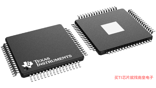
The TLK1501 is housed in a high performance, thermally enhanced, 64-pin VQFP PowerPAD package. Use of the PowerPAD package does not require any special considerations except to note that the PowerPAD, which is an exposed die pad on the bottom of the device, is a metallic thermal and electrical conductor. It is recommended that the TLK1501 PowerPAD be soldered to the thermal land on the board. All ac performance specifications in this data sheet are measured with the PowerPAD soldered to the test board.
The TLK1501 provides an internal loopback capability for self-test purposes. Serial data from the serializer is passed directly to the deserializer, allowing the protocol device a functional self-check of the physical interface.
The TLK1501 is designed to be hot plug capable. An on-chip power-on reset circuit holds the RX_CLK low during power up. This circuit also holds the parallel side output signal terminals during power up as well as DOUTTXP and DOUTTXN in a high-impedance state.
The TLK1501 has a loss of signal detection circuit for conditions where the incoming signal no longer has a sufficient voltage amplitude to keep the clock recovery circuit in lock.
To prevent a data bit error from causing a valid data packet from being interpreted as a comma and thus causing the erroneous word alignment by the comma detection circuit, the comma word alignment circuit is turned off after the link is properly established in TLK1501.
The TLK1501 allows users to implement redundant ports by connecting receive data bus terminals from two TLK1501 devices together. Asserting the LCKREFN to a low state causes the receive data bus terminals, RXD[0:15], RX_CLK and RX_ER, RX_DV/LOS to go to a high-impedance state. This places the device in a transmit-only mode, since the receiver is not tracking the data.
The TLK1501 uses a 2.5-V supply. The I/O section is 3 V compatible. With the 2.5-V supply the chipset is very power-efficient, consuming less than 360 mW typically. The TLK1501 is characterized for operation from –40°C to 85°C.
- Hot Plug Protection
- 0.6 to 1.5 Gigabits Per Second (Gbps) Serializer/Deserializer
- High-Performance 64-Pin VQFP Thermally Enhanced Package (PowerPAD?)
- 2.5 V Power Supply for Low Power Operation
- Programmable Voltage Output Swing on Serial Output
- Interfaces to Backplane, Copper Cables, or Optical Converters
- Rated for Industrial Temperature Range
- On-Chip 8-Bit/10-Bit (8B/10B) Encoding/Decoding, Comma Alignment, and Link Synchronization
- On-Chip PLL Provides Clock Synthesis From Low-Speed Reference
- Receiver Differential Input Thresholds 200 mV Minimum
- Typical Power: 250 mW
- Loss of Signal (LOS) Detection
- Ideal for High-Speed Backplane Interconnect and Point-to-Point Data Link
PowerPAD is a trademark of Texas Instruments.
- Operating temperature range (C)
- -40 to 85
TLK1501ΒΡΆξ’ϊ–ΆΚ≈”–ΘΚTLK1501IRCPΓΔTLK1501IRCPRΘ§“‘œ¬ «’β–©≤ζΤΖΒΡΙΊΦϋ≤Έ ΐΦΑΙΌΆχ≤…ΙΚ±®ΦέΘΚ
TLK1501IRCPΘ§ΙΛΉςΈ¬Ε»ΘΚ-40 to 85Θ§ΖβΉΑΘΚHVQFP (RCP)-64Θ§ΑϋΉΑ ΐΝΩMPQΘΚ160ΗωΘ§MSL Β»ΦΕ/ΜΊΝςΚΗΖε÷ΒΈ¬Ε»ΘΚLevel-3-260C-168 HRΘ§“ΐΫ≈ΕΤ≤ψ/ΚΗ«ρ≤ΡΝœΘΚNIPDAUΘ§TIΙΌΆχTLK1501IRCPΒΡ≈ζΝΩUSDΦέΗώΘΚ12.586Θ®1000+Θ©
TLK1501IRCPRΘ§ΙΛΉςΈ¬Ε»ΘΚ-40 to 85Θ§ΖβΉΑΘΚHVQFP (RCP)-64Θ§ΑϋΉΑ ΐΝΩMPQΘΚ1000ΗωΘ§MSL Β»ΦΕ/ΜΊΝςΚΗΖε÷ΒΈ¬Ε»ΘΚLevel-3-260C-168 HRΘ§“ΐΫ≈ΕΤ≤ψ/ΚΗ«ρ≤ΡΝœΘΚNIPDAUΘ§TIΙΌΆχTLK1501IRCPRΒΡ≈ζΝΩUSDΦέΗώΘΚ10.962Θ®1000+Θ©

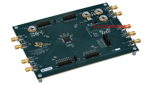
TLK1501EVM ΓΣ TLK1501 ¥°––Τς/Ϋβ¥°ΤςΤάΙάΡΘΩι
The TLK1501 serdes evaluatiom module (EVM) board is used to evaluate the TLK1501 device (VQFP) and associated optical interface (NetLight™) for point-to-point data transmission applications.
The board enables the designer to connect 50 ohm parallel buses to both transmitter and receiver connectors. (...)
PSPICE-FOR-TI ΓΣ ”Ο”Ύ TI …ηΦΤΚΆΡΘΡβΙΛΨΏΒΡ PSpice
PSpice for TI Ω…ΧαΙ©Αο÷ζΤάΙάΡΘΡβΒγ¬ΖΙΠΡήΒΡ…ηΦΤΚΆΖ¬’φΜΖΨ≥ΓΘ¥ΥΙΠΡήΤκ»ΪΒΡ…ηΦΤΚΆΖ¬’φΧΉΦΰ Ι”Ο Cadence ΒΡΡΘΡβΖ÷Έω“ΐ«φΓΘPSpice for TI Ω…ΟβΖ― Ι”ΟΘ§Αϋά®“ΒΡΎ≥§¥σΒΡΡΘ–ΆΩβ÷°“ΜΘ§Κ≠Η«Έ“Ο«ΒΡΡΘΡβΚΆΒγ‘¥≤ζΤΖœΒΝ–“‘ΦΑΨΪ―ΓΒΡΡΘΡβ––ΈΣΡΘ–ΆΓΘΫη÷ζ?PSpice for TI ΒΡ…ηΦΤΚΆΖ¬’φΜΖΨ≥ΦΑΤδΡΎ÷ΟΒΡΡΘ–ΆΩβΘ§ΡζΩ…Ε‘Η¥‘”ΒΡΜλΚœ–≈Κ≈…ηΦΤΫχ––Ζ¬’φΓΘ¥¥Ϋ®Άξ’ϊΒΡ÷’ΕΥ…η±Η…ηΦΤΚΆ‘≠–ΆΫβΨωΖΫΑΗΘ§»ΜΚσ‘ΌΫχ––≤ΦΨ÷ΚΆ÷Τ‘λΘ§Ω…ΥθΕΧ≤ζΤΖ…œ – ±Φδ≤ΔΫΒΒΆΩΣΖΔ≥…±ΨΓΘ
‘Ύ?PSpice for TI …ηΦΤΚΆΖ¬’φΙΛΨΏ÷–Θ§ΡζΩ…“‘Υ―Υς TI (...)
TINA-TI ΓΣ Μυ”Ύ SPICE ΒΡΡΘΡβΖ¬’φ≥Χ–ρ
TINA-TI ΧαΙ©ΝΥ SPICE Υυ”–ΒΡ¥ΪΆ≥÷±ΝςΓΔΥ≤Χ§ΚΆΤΒ”ρΖ÷Έω“‘ΦΑΗϋΕύΓΘTINA ΨΏ”–ΙψΖΚΒΡΚσ¥ΠάμΙΠΡήΘ§‘ –μΡζΑ¥’’œΘΆϊΒΡΖΫ Ϋ…η÷ΟΫαΙϊΒΡΗώ ΫΓΘ–ιΡβ“«Τς‘ –μΡζ―Γ‘ώ δ»κ≤®–ΈΓΔΧΫ’κΒγ¬ΖΫΎΒψΒγ―ΙΚΆ≤®–ΈΓΘTINA ΒΡ‘≠άμΆΦ≤ΕΜώΖ«≥Θ÷±Ιέ - ’φ’ΐΒΡΓΑΩλΥΌ»κΟ≈Γ±ΓΘTINA-TI Α≤ΉΑ–η“Σ¥σ‘Φ 500MBΓΘ÷±Ϋ”Α≤ΉΑΘ§»γΙϊœκ–Ε‘Ί“≤Κή»ί“ΉΓΘΈ“Ο«œύ–≈ΡζΩœΕ®ΜαΑ°≤Μ Ά ÷ΓΘ
TINA «Β¬÷ί“«Τς (TI) Ή®”–ΒΡ DesignSoft ≤ζΤΖΓΘΗΟΟβΖ―Αφ±ΨΨΏ”–Άξ’ϊΒΡΙΠΡήΘ§ΒΪ≤Μ÷ß≥÷Άξ’ϊΑφ TINA ΥυΧαΙ©ΒΡΡ≥–©ΤδΥϊΙΠΡήΓΘ
»γ–ηΜώ»ΓΩ…”Ο TINA-TI ΡΘ–ΆΒΡΆξ’ϊΝ–±μΘ§«κ≤Έ‘ΡΘΚSpiceRack - Άξ’ϊΝ–±μ
–η“Σ HSpice (...)


