- 制造厂商:TI
- 产品类别:数据转换器
- 技术类目:模数转换器 (ADC) - 精密模数转换器 (<=10MSPS)
- 功能描述:具有串行控制和 8 个模拟输入的汽车类低压 10 位模数转换器
- 点击这里打开及下载TLV1548-Q1的技术文档资料
- TI代理渠道,提供当日发货、严格的质量标准,满足您的目标价格

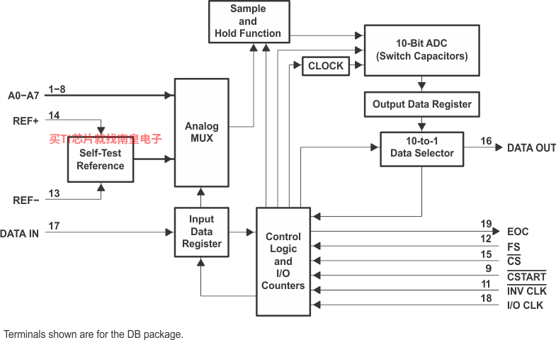
The TLV1548 is a CMOS 10-bit switched-capacitor successive-approximation (SAR) analog-to-digital (A/D) converter. The device has a chip select (CS), input-output clock (I/O CLK), data input (DATA IN) and serial data output (DATA OUT) that provides a direct 4-wire synchronous serial peripheral interface (SPI™, QSPI™) port of a host microprocessor. When interfacing with a TMS320 DSP, an additional frame sync signal (FS) indicates the start of a serial data frame. The device allows high-speed data transfers from the host. The INV CLK\ input provides further timing flexibility for the serial interface.
In addition to a high-speed converter and versatile control capability, the device has an on-chip 11-channel multiplexer that can select any one of eight analog inputs or any one of three internal self-test voltages. The sample-and-hold function is automatic except for the extended sampling cycle, where the sampling cycle is started by the falling edge of asynchronous CSTART. At the end of the A/D conversion, the end-of-conversion (EOC) output goes high to indicate that the conversion is complete. The TLV1548 is designed to operate with a wide range of supply voltages with very low power consumption. The power saving feature is further enhanced with a software-programmed power-down mode and conversion rate. The converter incorporated in the device features differential high-impedance reference inputs that facilitate ratiometric conversion, scaling, and isolation of analog circuitry from logic and supply noise. A switched-capacitor design allows low-error conversion over the full operating temperature range.
The TLV1548 has eight analog input channels. The TLV1548Q is characterized for operation over the full automotive temperature range of –40°C to 125°C.
- Qualified for Automotive Applications
- ESD Protection Exceeds 2000 V Per MIL-STD-883, Method 3015; Exceeds 200 V Using Machine Model (C = 200 pF, R = 0)
- Conversion Time ≤ 10 s
- 10-Bit-Resolution ADC
- Programmable Power-Down Mode . . . 1 A
- Wide Range Single-Supply Operation of 2.7 V dc to 5.5 V dc
- Analog Input Range of 0 V to VCC
- Built-in Analog Multiplexer with 8 Analog Input Channels
- TMS320 DSP and Microprocessor SPI and QSPI Compatible Serial Interfaces
- End-of-Conversion (EOC) Flag
- Inherent Sample-and-Hold Function
- Built-In Self-Test Modes
- Programmable Power and Conversion Rate
- Asynchronous Start of Conversion for Extended Sampling
- Hardware I/O Clock Phase Adjust Input
SPI and QSPI are registered trademarks of Motorola, Inc.
- Resolution (Bits)
- 10
- Number of input channels
- 8
- Sample rate (Max) (kSPS)
- 85
- Interface type
- SPI
- Architecture
- SAR
- Input type
- Single-Ended
- Multi-channel configuration
- Multiplexed
- Rating
- Automotive
- Reference mode
- Ext
- Input range (Max) (V)
- 5.5
- Input range (Min) (V)
- 0
- Features
- Operating temperature range (C)
- -40 to 125
- Power consumption (Typ) (mW)
- 1.05
- Analog voltage AVDD (Min) (V)
- 2.7
- Analog voltage AVDD (Max) (V)
- 5.5
- INL (Max) (+/-LSB)
- 1
- Digital supply (Min) (V)
- 2.7
- Digital supply (Max) (V)
- 5.5
TLV1548-Q1的完整型号有:TLV1548QDBRG4Q1、TLV1548QDBRQ1,以下是这些产品的关键参数及官网采购报价:
TLV1548QDBRG4Q1,工作温度:-40 to 125,封装:SSOP (DB)-20,包装数量MPQ:2000个,MSL 等级/回流焊峰值温度:Level-1-260C-UNLIM,引脚镀层/焊球材料:NIPDAU,TI官网TLV1548QDBRG4Q1的批量USD价格:3.383(1000+)
TLV1548QDBRQ1,工作温度:-40 to 125,封装:SSOP (DB)-20,包装数量MPQ:2000个,MSL 等级/回流焊峰值温度:Level-1-260C-UNLIM,引脚镀层/焊球材料:NIPDAU,TI官网TLV1548QDBRQ1的批量USD价格:3.383(1000+)

PSPICE-FOR-TI 适用于 TI 设计和模拟工具的 PSpice
PSpice for TI 可提供帮助评估模拟电路功能的设计和仿真环境。此功能齐全的设计和仿真套件使用 Cadence 的模拟分析引擎。PSpice for TI 可免费使用,包括业内超大的模型库之一,涵盖我们的模拟和电源产品系列以及精选的模拟行为模型。借助PSpice for TI 的设计和仿真环境及其内置的模型库,您可对复杂的混合信号设计进行仿真。创建完整的终端设备设计和原型解决方案,然后再进行布局和制造,可缩短产品上市时间并降低开发成本。
在PSpice for TI 设计和仿真工具中,您可以搜索 TI (...)
TINA-TI 基于 SPICE 的模拟仿真程序
TINA-TI 提供了 SPICE 所有的传统直流、瞬态和频域分析以及更多。TINA 具有广泛的后处理功能,允许您按照希望的方式设置结果的格式。虚拟仪器允许您选择输入波形、探针电路节点电压和波形。TINA 的原理图捕获非常直观 - 真正的“快速入门”。TINA-TI 安装需要大约 500MB。直接安装,如果想卸载也很容易。我们相信您肯定会爱不释手。
TINA 是德州仪器 (TI) 专有的 DesignSoft 产品。该免费版本具有完整的功能,但不支持完整版 TINA 所提供的某些其他功能。
如需获取可用 TINA-TI 模型的完整列表,请参阅:SpiceRack - 完整列表
需要 HSpice (...)
ADC-INPUT-CALC Analog-to-digital converter (ADC) input driver design tool supporting multiple input types
ADC-INPUT-CALC 是一种在线工具,可为设计模数转换器 (ADC) 的输入缓冲器提供支持。它提供 24 种不同的基于运算放大器的缓冲器电路,这些电路可用于驱动 ADC 输入。可用拓扑涵盖差分单端和变压器耦合输入设计。支持交流耦合和直流耦合设计以及单电源和双电源拓扑。提供两种模式:初学者模式和专家模式。在初学者模式中,设计人员先回答一系列问题,然后会看到解决方案原理图,在某些情况下,还会看到解决方案的可选版本。在专家模式下,设计人员会看到用方框图形式显示的所有 24 (...)ANALOG-ENGINEER-CALC 模拟工程师计算器
模拟工程师计算器旨在加快模拟电路设计工程师经常使用的许多重复性计算。该基于 PC 的工具提供图形界面,其中显示各种常见计算的列表(从使用反馈电阻器设置运算放大器增益到为稳定模数转换器 (ADC) 驱动器缓冲器电路选择合适的电路设计元件)。除了可用作单独的工具之外,该计算器还能够很好地与模拟工程师口袋参考书中所述的概念配合使用。 lock = 需要出口许可(1分钟)