

- 制造厂商:TI(德州仪器,Texas Instruments)
- 产品类别:数据转换器
- 技术类目:模数转换器 (ADC) - 精密模数转换器 (<=10MSPS)
- 功能描述:10 位四通道(可配置)2MSPS ADC,具有多路可编程分辨率与速度/转换模式,自动工作
- 点击这里打开及下载TLV1562的技术文档资料
- TI代理渠道,提供当日发货、严格的质量标准,满足您的目标价格

The TLV1562 is a 10-bit CMOS low-power, high-speed programmable resolution analog-to-digital converter based on a low-power recyclic architecture. The unique architecture delivers a throughput up to 2 MSPS (million samples per second) at 10-bit resolution. The programmable resolution allows a higher conversion throughput as a tradeoff of lower resolution. A high speed 3-state parallel port directly interfaces to a digital signal processor (DSP) or microprocessor (uP) system data bus. D0 through D9 are the digital output terminals with D0 being the least significant bit (LSB). The TLV1562 is designed to operate for a wide range of supply voltages (2.7 V to 5.5 V) with very low power consumption (11 mA maximum at 5.5 V, 10 MHz CLKIN). The power saving feature is further enhanced with a software power-down feature (1 uA maximum) and auto power-down (1 uA maximum) feature.
Many programmable features make this device a flexible general-purpose data converter. The device can be configured as either four single-ended inputs to maximize the capacity or two differential inputs to improve noise immunity. The internal system clock (SYSCLK) may come from either an internally generated OSC or an external clock source (CLKIN). Four different modes of conversion are available for different applications. The interrupt driven modes are mostly suitable for asynchronous applications, while the continuous modes take advantage of the high speed nature of a pipelined architecture. A pair of built-in sample-and-hold amplifiers allow simultaneous sampling of two input channels. This makes the TLV1562 perfect for communication applications. Conversion is started by the RD\ signal, which can also be used for reading data, to maximize the throughput. Conversion can be started either by the RD\ or CSTART\ signal when the device is operating in the interrupt-driven modes. The dedicated conversion start pin, CSTART\, provides a mechanism to simultaneously sample and convert multiple channels when multiple converters are used in an application.
The converter incorporates a pair of differential high-impedance reference inputs that facilitate ratiometric conversion, scaling, and isolation of analog circuitry from logic and supply noise. Other features such as low input capacitance (10 pF) and very wide input bandwidth (75 MHz) make this device a perfect digital signal processing (DSP) companion for mobile communication applications. A switched-capacitor design allows low-error conversion over the full operating free-air temperature range.
The features that make this device truly a DSP friendly converter include: 1) programmable continuous conversion modes, 2) programmable 2s complement output code format, and 3) programmable resolution. The TLV1562 is offered in both 28-pin TSSOP and SOIC packages. The TLV1562C is characterized for operation from 0°C to 70°C. The TLV1562I is characterized for operation over the full industrial temperature range of -40°C to 85°C.
- 2 MSPS Max Throughput at 10 Bit (Single Channel), ±1 LSB DNL, ±1 LSB INL MAX
- 3 MSPS Max Throughput at 8 Bit (Single Channel), ±1 LSB DNL, ±1 LSB INL MAX
- 7 MSPS Max Throughput at 4 Bit (Single Channel), ±0.4 LSB DNL, ±0.4 LSB INL MAX
- No Missing Code for External Clock Up to 15 MHz at 5.5 V, 12 MHz at 2.7 V
- ENOB 9.4 Bit, SINAD 57.8 dB, SFDR -70.8 dB, THD -68.8 dB, at fi = 800 kHz, 10 Bit
- Wide Input Bandwidth for Undersampling (75 MHz at 1 dB, >120 MHz at -3 dB) at Rs = 1 k
- Software Programmable Power Down, (1 uA), Auto Powerdown (120 uA)
- Single Wide Range Supply 2.7 VDC to 5.5 VDC
- Low Supply Current 11 mA at 5.5 V, 10 MHz; 7 mA at 2.7 V, 8 MHz Operating
- Simultaneous Sample and Hold:
- Dual Sample and Hold Matched Channels
- Multi Chip Simultaneous Sample and Hold Capable
- Programmable Conversion Modes: Interrupt-Driven for Shorter Latency Continuous Modes Optimized for MIPS Sensitive DSP Solutions
- Built-In Internal/System Mid-Scale Error Calibration
- Built-In Mux With 2 Differential or 4 Single-Ended Input Channels
- Low Input Capacitance (10 pF Max Fixed, 1 pF Max Switching)
- DSP/u P-Compatible Parallel Interface
- Resolution (Bits)
- 10
- Number of input channels
- 4
- Sample rate (Max) (kSPS)
- 2000
- Interface type
- Parallel
- Architecture
- Pipeline
- Input type
- Differential, Single-Ended
- Multi-channel configuration
- Multiplexed
- Rating
- Catalog
- Reference mode
- Ext
- Input range (Max) (V)
- 3
- Input range (Min) (V)
- 0.8
- Features
- Oscillator
- Operating temperature range (C)
- -40 to 85, 0 to 70
- Power consumption (Typ) (mW)
- 13.5
- Analog voltage AVDD (Min) (V)
- 2.7
- SNR (dB)
- 58.1
- Analog voltage AVDD (Max) (V)
- 5.5
- INL (Max) (+/-LSB)
- 1
- Digital supply (Min) (V)
- 2.7
- Digital supply (Max) (V)
- 5.5
TLV1562的完整型号有:TLV1562CPW、TLV1562IDW、TLV1562IPW,以下是这些产品的关键参数及官网采购报价:
TLV1562CPW,工作温度:0 to 70,封装:TSSOP (PW)-28,包装数量MPQ:50个,MSL 等级/回流焊峰值温度:Level-1-260C-UNLIM,引脚镀层/焊球材料:NIPDAU,TI官网TLV1562CPW的批量USD价格:5.775(1000+)
TLV1562IDW,工作温度:-40 to 85,封装:SOIC (DW)-28,包装数量MPQ:20个,MSL 等级/回流焊峰值温度:Level-1-260C-UNLIM,引脚镀层/焊球材料:NIPDAU,TI官网TLV1562IDW的批量USD价格:5.775(1000+)
TLV1562IPW,工作温度:-40 to 85,封装:TSSOP (PW)-28,包装数量MPQ:50个,MSL 等级/回流焊峰值温度:Level-1-260C-UNLIM,引脚镀层/焊球材料:NIPDAU,TI官网TLV1562IPW的批量USD价格:5.775(1000+)

PSPICE-FOR-TI 适用于 TI 设计和模拟工具的 PSpice
PSpice for TI 可提供帮助评估模拟电路功能的设计和仿真环境。此功能齐全的设计和仿真套件使用 Cadence 的模拟分析引擎。PSpice for TI 可免费使用,包括业内超大的模型库之一,涵盖我们的模拟和电源产品系列以及精选的模拟行为模型。借助PSpice for TI 的设计和仿真环境及其内置的模型库,您可对复杂的混合信号设计进行仿真。创建完整的终端设备设计和原型解决方案,然后再进行布局和制造,可缩短产品上市时间并降低开发成本。
在PSpice for TI 设计和仿真工具中,您可以搜索 TI (...)
TINA-TI 基于 SPICE 的模拟仿真程序
TINA-TI 提供了 SPICE 所有的传统直流、瞬态和频域分析以及更多。TINA 具有广泛的后处理功能,允许您按照希望的方式设置结果的格式。虚拟仪器允许您选择输入波形、探针电路节点电压和波形。TINA 的原理图捕获非常直观 - 真正的“快速入门”。TINA-TI 安装需要大约 500MB。直接安装,如果想卸载也很容易。我们相信您肯定会爱不释手。
TINA 是德州仪器 (TI) 专有的 DesignSoft 产品。该免费版本具有完整的功能,但不支持完整版 TINA 所提供的某些其他功能。
如需获取可用 TINA-TI 模型的完整列表,请参阅:SpiceRack - 完整列表
需要 HSpice (...)
ADC-INPUT-CALC Analog-to-digital converter (ADC) input driver design tool supporting multiple input types
ADC-INPUT-CALC 是一种在线工具,可为设计模数转换器 (ADC) 的输入缓冲器提供支持。它提供 24 种不同的基于运算放大器的缓冲器电路,这些电路可用于驱动 ADC 输入。可用拓扑涵盖差分单端和变压器耦合输入设计。支持交流耦合和直流耦合设计以及单电源和双电源拓扑。提供两种模式:初学者模式和专家模式。在初学者模式中,设计人员先回答一系列问题,然后会看到解决方案原理图,在某些情况下,还会看到解决方案的可选版本。在专家模式下,设计人员会看到用方框图形式显示的所有 24 (...)ANALOG-ENGINEER-CALC 模拟工程师计算器
模拟工程师计算器旨在加快模拟电路设计工程师经常使用的许多重复性计算。该基于 PC 的工具提供图形界面,其中显示各种常见计算的列表(从使用反馈电阻器设置运算放大器增益到为稳定模数转换器 (ADC) 驱动器缓冲器电路选择合适的电路设计元件)。除了可用作单独的工具之外,该计算器还能够很好地与模拟工程师口袋参考书中所述的概念配合使用。 lock = 需要出口许可(1分钟)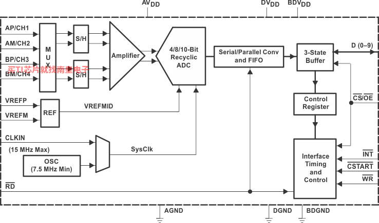
- SN65C23243
- LM3519
- ISO7240CF-Q1
- F28M35M22C
- HD3SS212
- TL971-Q1
- ADS7052
- TPS61072
- LMV822-N-Q1
- UCC21750
- MSP430F5631
- SN74ABT8652
- TPS65141
- MSP430F6745
- SN54LS595
- CSD87352Q5D
- LMV881
- TAS3208
- TPS62403
- TPS56C231
- THS4551RGTEVM
- SN74AC563NSR
- TLC2551EVM
- CD4013BPW
- CC2540F256RHAR
- SN74LS283D
- OPA2170AIDR
- SN74ALVC162334DL
- SN74F157AD
- PT6722A
- F28M35E50C1RFPT
- TCAN1051GVDRBTQ1
- LM555CMM/NOPB
- LM4120AIM5-3.3
- UCC2837D
- DAC8830ICDR
- UCD90320EVM-783
- F28P650DK9NMR
- TLV341AIDBVTE4
- TPS3305-18DR
