- 制造厂商:TI
- 产品类别:电源管理
- 技术类目:直流/直流开关稳压器 - 降压稳压器
- 功能描述:采用 2x2 SON 封装的 3MHz、2A 降压转换器
- 点击这里打开及下载TLV62065的技术文档资料
- TI代理渠道,提供当日发货、严格的质量标准,满足您的目标价格

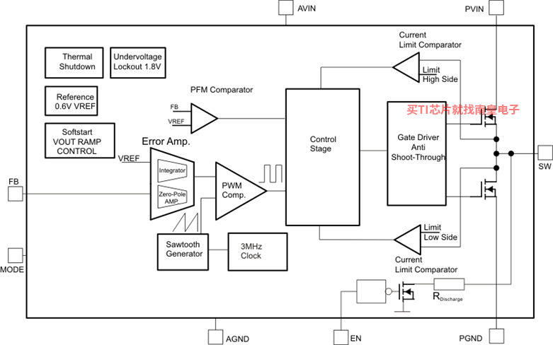
The TLV62065 device is a high efficiency synchronous step-down DC–DC converter. It provides up to 2-A output current.
With an input voltage range of 2.9 V to 5.5 V, the device is a perfect fit for power conversion from a 5-V or 3.3-V system supply rail. The TLV62065 operates at 3-MHz fixed frequency and enters power-save mode operation at light load currents to maintain high efficiency over the entire load current range. For low noise applications, TLV62065 can be forced into fixed frequency PWM mode by pulling the MODE pin high.
In the shutdown mode, the current consumption is reduced to less than 1 μA and an internal circuit discharges the output capacitor.
TLV62065 operates with a 1-µH inductor and 10-µF output capacitor.
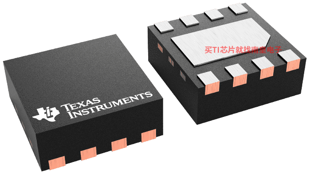
The TLV62065 is available in a small 2 mm × 2 mm × 0.75 mm 8-pin WSON package.
- VIN Range from 2.9 V to 5.5 V
- Up to 97% Efficiency
- Power-Save Mode / 3-MHz Fixed PWM Mode
- Output Voltage Accuracy in PWM Mode ±2.0%
- Output Capacitor Discharge Function
- Typical 18-μA Quiescent Current
- 100% Duty Cycle for Lowest Dropout
- Available in a 2 mm × 2 mm × 0.75 mm WSON
- APPLICATIONS
- Point-of-Load (POL)
- Notebooks, Pocket PCs
- Portable Media Players
- Set-Top Boxes
All other trademarks are the property of their respective owners
- Vin (Min) (V)
- 2.9
- Vin (Max) (V)
- 5.5
- Vout (Min) (V)
- 0.8
- Vout (Max) (V)
- 5.5
- Iout (Max) (A)
- 2
- Iq (Typ) (uA)
- 18000
- Switching frequency (Min) (kHz)
- 2600
- Switching frequency (Max) (kHz)
- 3400
- Features
- Enable, Forced PWM, Light Load Efficiency, Output Discharge, Spread Spectrum, Synchronous Rectification, UVLO Fixed
- Rating
- Catalog
- Regulated outputs (#)
- 1
- Control mode
- Voltage Mode
- Duty cycle (Max) (%)
- 100
TLV62065的完整型号有:TLV62065DSGR、TLV62065DSGT,以下是这些产品的关键参数及官网采购报价:
TLV62065DSGR,工作温度:-40 to 85,封装:WSON (DSG)-8,包装数量MPQ:3000个,MSL 等级/回流焊峰值温度:Level-2-260C-1 YEAR,引脚镀层/焊球材料:NIPDAUAG,TI官网TLV62065DSGR的批量USD价格:.542(1000+)
TLV62065DSGT,工作温度:-40 to 85,封装:WSON (DSG)-8,包装数量MPQ:250个,MSL 等级/回流焊峰值温度:Level-2-260C-1 YEAR,引脚镀层/焊球材料:NIPDAUAG,TI官网TLV62065DSGT的批量USD价格:.65(1000+)

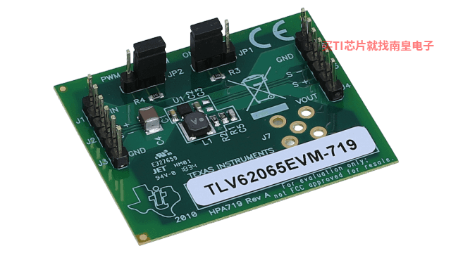
TLV62065EVM-719 ― 采用 2x2 SON 封装的 TLV62065 3MHz、2A 降压转换器的评估模块
TLV62065EVM-719 是一个完全组装且经过测试的平台,用于评估 TLV62065 2.0A 降压转换器的性能。本用户指南文档包含原理图、印制电路板 (PCB) 布局、物料清单和测试数据。除非特别说明,否则本文档内的缩写词 EVM、TLV62065EVM 以及术语“评估模块”均代表 TLV62065EVM-719。
TPS62065 Unencrypted PSpice Transient Model Package (Rev. B)
PSpice for TI 可提供帮助评估模拟电路功能的设计和仿真环境。此功能齐全的设计和仿真套件使用 Cadence 的模拟分析引擎。PSpice for TI 可免费使用,包括业内超大的模型库之一,涵盖我们的模拟和电源产品系列以及精选的模拟行为模型。借助?PSpice for TI 的设计和仿真环境及其内置的模型库,您可对复杂的混合信号设计进行仿真。创建完整的终端设备设计和原型解决方案,然后再进行布局和制造,可缩短产品上市时间并降低开发成本。
在?PSpice for TI 设计和仿真工具中,您可以搜索 TI (...)
Design Tool for Output Voltage Adjustment Using a DAC
In today’s start-stop systems, it is common for battery voltages to dip well below the nominal 12V rating. PMP8903 represents a very common start-stop application where that battery voltage can drop as low as 5V, and a 5V output is still needed for CAN and also as an intermediate bus. This (...)