- 制造厂商:TI
- 产品类别:微控制器 (MCU) 和处理器
- 技术类目:处理器 - 数字信号处理器 (DSP)
- 功能描述:C64x+ 定点 DSP- 高达 600MHz、16/8 位 EMIFA、32/16 位 DDR2
- 点击这里打开及下载TMS320C6424Q的技术文档资料
- TI代理渠道,提供当日发货、严格的质量标准,满足您的目标价格

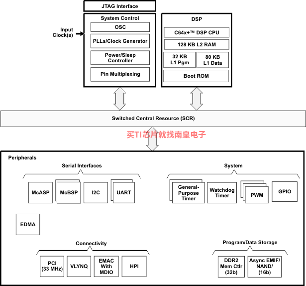
The TMS320C64x+™ DSPs (including the TMS320C6424 device) are the highest-performance fixed-point DSP generation in the TMS320C6000™ DSP platform. The C6424 device is based on the third-generation high-performance, advanced VelociTI™ very-long-instruction-word (VLIW) architecture developed by Texas Instruments (TI), making these DSPs an excellent choice for digital signal processor applications. The C64x+™ devices are upward code-compatible from previous devices that are part of the C6000™ DSP platform. The C64x™ DSPs support added functionality and have an expanded instruction set from previous devices.
Any reference to the C64x DSP or C64x CPU also applies, unless otherwise noted, to the C64x+ DSP and C64x+ CPU, respectively.
With performance of up to 4800 million instructions per second (MIPS) at a clock rate of 600 MHz, the C64x+ core offers solutions to high-performance DSP programming challenges. The DSP core possesses the operational flexibility of high-speed controllers and the numerical capability of array processors. The C64x+ DSP core processor has 64 general-purpose registers of 32-bit word length and eight highly independent functional units-two multipliers for a 32-bit result and six arithmetic logic units (ALUs). The eight functional units include instructions to accelerate the performance in telecom, audio, and industrial applications. The DSP core can produce four 16-bit multiply-accumulates (MACs) per cycle for a total of 2400 million MACs per second (MMACS), or eight 8-bit MACs per cycle for a total of 4800 MMACS. For more details on the C64x+ DSP, see the TMS320C64x/C64x+ DSP CPU and Instruction Set Reference Guide (literature number SPRU732).
The C6424 also has application-specific hardware logic, on-chip memory, and additional on-chip peripherals similar to the other C6000 DSP platform devices. The C6424 core uses a two-level cache-based architecture. The Level 1 program memory/cache (L1P) consists of a 256K-bit memory space that can be configured as mapped memory or direct mapped cache, and the Level 1 data (L1D) consists of a 640K-bit memory space–384K-bit of which is mapped memory and 256K-bit of which can be configured as mapped memory or 2-way set-associative cache. The Level 2 memory/cache (L2) consists of a 1M-bit memory space that is shared between program and data space. L2 memory can be configured as mapped memory, cache, or combinations of the two.
The peripheral set includes: a 10/100 Mb/s Ethernet MAC (EMAC) with a management data input/output (MDIO) module; a 4-bit transmit, 4-bit receive VLYNQ interface; an inter-integrated circuit (I2C) Bus interface; two multichannel buffered serial ports (McBSPs); a multichannel audio serial port (McASP0) with 4 serializers; 2 64-bit general-purpose timers each configurable as 2 independent 32-bit timers; 1 64-bit watchdog timer; a user-configurable 16-bit host-port interface (HPI); up to 111-pins of general-purposeinput/output (GPIO) with programmable interrupt/event generation modes, multiplexed with other peripherals; 2 UARTs with hardware handshaking support on 1 UART; 3 pulse width modulator (PWM) peripherals; 1 peripheral component interconnect (PCI) [33 MHz]; and 2 glueless external memory interfaces: an asynchronous external memory interface (EMIFA) for slower memories/peripherals, and a higher speed synchronous memory interface for DDR2.
The Ethernet Media Access Controller (EMAC) provides an efficient interface between the C6424 and the network. The C6424 EMAC supports 10Base-T and 100Base-TX, or 10 Mbits/second (Mbps) and 100 Mbps in either half- or full-duplex mode, with hardware flow control and quality of service (QOS) support.
The Management Data Input/Output (MDIO) module continuously polls all 32 MDIO addresses in order to enumerate all PHY devices in the system.
The I2C and VLYNQ ports allow C6424 to easily control peripheral devices and/or communicate with host processors.
The rich peripheral set provides the ability to control external peripheral devices and communicate with external processors. For details on each of the peripherals, see the related sections later in this document and the associated peripheral reference guides.
The C6424 has a complete set of development tools. These include C compilers, a DSP assembly optimizer to simplify programming and scheduling, and a Windows™ debugger interface for visibility into source code execution.
- High-Performance Digital Signal Processor (C6424)
- 2.5-, 2-, 1.67, 1.43-ns Instruction Cycle Time
- 400-, 500-, 600-MHz C64x+? Clock Rate
- Eight 32-Bit C64x+ Instructions/Cycle
- 3200, 4000, 4800, 5600 MIPS
- Fully Software-Compatible With C64x
- Commercial and Automotive (Q or S suffix)Grades
- Low-Power Device (L suffix)
- VelociTI.2? Extensions to VelociTI? Advanced Very-Long-Instruction-Word (VLIW) TMS320C64x+? DSP Core
- Eight Highly Independent Functional Units With VelociTI.2 Extensions:
- Six ALUs (32-/40-Bit), Each Supports Single 32-Bit, Dual 16-Bit, or Quad 8-Bit Arithmetic per Clock Cycle
- Two Multipliers Support Four 16 × 16-Bit Multiplies (32-Bit Results) per Clock Cycle or Eight 8 × 8-Bit Multiplies (16-Bit Results) per Clock Cycle
- Load-Store Architecture With Non-Aligned Support
- 64 32-Bit General-Purpose Registers
- Instruction Packing Reduces Code Size
- All Instructions Conditional
- Additional C64x+? Enhancements
- Protected Mode Operation
- Exceptions Support for Error Detection and Program Redirection
- Hardware Support for Modulo Loop Auto-Focus Module Operation
- Eight Highly Independent Functional Units With VelociTI.2 Extensions:
- C64x+ Instruction Set Features
- Byte-Addressable (8-/16-/32-/64-Bit Data)
- 8-Bit Overflow Protection
- Bit-Field Extract, Set, Clear
- Normalization, Saturation, Bit-Counting
- VelociTI.2 Increased Orthogonality
- C64x+ Extensions
- Compact 16-bit Instructions
- Additional Instructions to Support Complex Multiplies
- C64x+ L1/L2 Memory Architecture
- 256K-Bit (32K-Byte) L1P Program RAM/Cache [Flexible Allocation]
- 640K-Bit (80K-Byte) L1D Data RAM/Cache [Flexible Allocation]
- 1M-Bit (128K-Byte) L2 Unified Mapped RAM/Cache [Flexible Allocation]
- Endianess: Supports Both Little Endian and Big Endian
- External Memory Interfaces (EMIFs)
- 32-Bit DDR2 SDRAM Memory Controller With 256M-Byte Address Space (1.8-V I/O)
- Supports up to 333-MHz (data rate) bus and interfaces to DDR2-400 SDRAM
- Asynchronous 16-Bit Wide EMIF (EMIFA) With up to 128M-Byte Address Reach
- Flash Memory Interfaces
- NOR (8-/16-Bit-Wide Data)
- NAND (8-/16-Bit-Wide Data)
- Flash Memory Interfaces
- 32-Bit DDR2 SDRAM Memory Controller With 256M-Byte Address Space (1.8-V I/O)
- Enhanced Direct-Memory-Access (EDMA) Controller (64 Independent Channels)
- Two 64-Bit General-Purpose Timers (Each Configurable as Two 32-Bit Timers)
- One 64-Bit Watch Dog Timer
- Two UARTs (One with RTS and CTS Flow Control)
- Master/Slave Inter-Integrated Circuit (I2C Bus?)
- Two Multichannel Buffered Serial Ports (McBSPs)
- I2S and TDM
- AC97 Audio Codec Interface
- SPI
- Standard Voice Codec Interface (AIC12)
- Telecom Interfaces - ST-Bus, H-100
- 128 Channel Mode
- Multichannel Audio Serial Port (McASP0)
- Four Serializers and SPDIF (DIT) Mode
- 16-Bit Host-Port Interface (HPI)
- 32-Bit 33-MHz, 3.3-V Peripheral Component Interconnect (PCI) Master/Slave Interface
- 10/100 Mb/s Ethernet MAC (EMAC)
- IEEE 802.3 Compliant
- Supports Multiple Media Independent Interfaces (MII, RMII)
- Management Data Input/Output (MDIO) Module
- VLYNQ? Interface (FPGA Interface)
- Three Pulse Width Modulator (PWM) Outputs
- On-Chip ROM Bootloader
- Individual Power-Savings Modes
- Flexible PLL Clock Generators
- IEEE-1149.1 (JTAG?) Boundary-Scan-Compatible
- Up to 111 General-Purpose I/O (GPIO) Pins (Multiplexed With Other Device Functions)
- Packages:
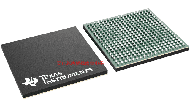
- 361-Pin Pb-Free PBGA Package (ZWT Suffix), 0.8-mm Ball Pitch
- 376-Pin Plastic BGA Package (ZDU Suffix), 1.0-mm Ball Pitch
- 0.09-μm/6-Level Cu Metal Process (CMOS)
- 3.3-V and 1.8-V I/O, 1.2-V Internal (-7/-6/-5/-4/-Q6/-Q5/-Q4)
- 3.3-V and 1.8-V I/O, 1.05-V Internal (-7/-6/-5/-4/-L/-Q5)
- APPLICATIONS
- Telecom
- Audio
- Industrial Applications
- Community Reesources
- TI E2E Community
- TI Embedded Processors Wiki
All trademarks are the property of their respective owners.
- DSP
- 1 C64x+
- DSP MHz (Max)
- 400, 500, 600
- CPU
- 32-/64-bit
- Ethernet MAC
- 10/100
- Rating
- Automotive
- Operating temperature range (C)
- -40 to 125
TMS320C6424Q的完整型号有:TMS320C6424ZDUQ5、TMS320C6424ZDUQ6、TMS320C6424ZWTQ5、TMS320C6424ZWTQ6,以下是这些产品的关键参数及官网采购报价:
TMS320C6424ZDUQ5,工作温度:-40 to 125,封装:BGA (ZDU)-376,包装数量MPQ:60个,MSL 等级/回流焊峰值温度:Level-3-260C-168 HR,引脚镀层/焊球材料:SNAGCU,TI官网TMS320C6424ZDUQ5的批量USD价格:22.777(1000+)
TMS320C6424ZDUQ6,工作温度:-40 to 125,封装:BGA (ZDU)-376,包装数量MPQ:60个,MSL 等级/回流焊峰值温度:Level-3-260C-168 HR,引脚镀层/焊球材料:SNAGCU,TI官网TMS320C6424ZDUQ6的批量USD价格:27.803(1000+)
TMS320C6424ZWTQ5,工作温度:-40 to 125,封装:NFBGA (ZWT)-361,包装数量MPQ:90个,MSL 等级/回流焊峰值温度:Level-3-260C-168 HR,引脚镀层/焊球材料:SNAGCU,TI官网TMS320C6424ZWTQ5的批量USD价格:22.777(1000+)
TMS320C6424ZWTQ6,工作温度:-40 to 125,封装:NFBGA (ZWT)-361,包装数量MPQ:90个,MSL 等级/回流焊峰值温度:Level-3-260C-168 HR,引脚镀层/焊球材料:SNAGCU,TI官网TMS320C6424ZWTQ6的批量USD价格:27.803(1000+)

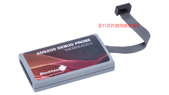
TMDSEMU200-U ― Spectrum Digital XDS200 USB 仿真器
Spectrum Digital XDS200 是最新 XDS200 系列 TI 处理器调试探针(仿真器)的首个模型。XDS200 系列拥有超低成本 XDS100 与高性能 XDS560v2 之间的低成本与高性能的完美平衡。此外,对于带有嵌入式缓冲跟踪器 (ETB) 的所有 ARM 和 DSP 处理器,所有 XDS 调试探针均支持内核和系统跟踪。
Spectrum Digital XDS200 通过 TI 20 引脚连接器(带有适合 TI 14 引脚、TI 10 引脚和 ARM 20 引脚的多个适配器)连接到目标板,而通过 USB2.0 高速连接 (480Mbps) 连接到主机 PC。要在主机 (...)
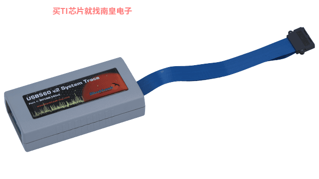
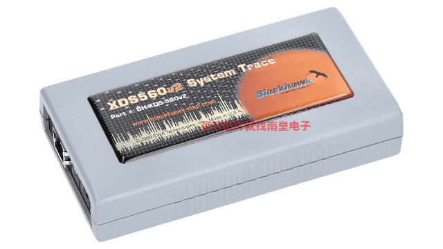
TMDSEMU560V2STM-U ― Blackhawk XDS560v2 系统跟踪 USB 仿真器
XDS560v2 System Trace 是 XDS560v2 系列高性能 TI 处理器调试探针(仿真器)的第一种型号。XDS560v2 是 XDS 系列调试探针中性能最高的一款,同时支持传统 JTAG 标准 (IEEE1149.1) 和 cJTAG (IEEE1149.7)。
XDS560v2 System Trace 在其巨大的外部存储器缓冲区中加入了系统引脚跟踪。这种外部存储器缓冲区适用于指定的 TI 器件,通过捕获相关器件级信息,获得准确的总线性能活动和吞吐量,并对内核和外设进行电源管理。此外,对于带有嵌入式缓冲跟踪器 (ETB) 的所有 ARM 和 DSP 处理器,所有 XDS (...)
TMDSEMU560V2STM-UE ― Spectrum Digital XDS560v2 系统跟踪 USB 和以太网
XDS560v2 System Trace 是 XDS560v2 系列高性能 TI 处理器调试探针(仿真器)的第一种型号。XDS560v2 是 XDS 系列调试探针中性能最高的一款,同时支持传统 JTAG 标准 (IEEE1149.1) 和 cJTAG (IEEE1149.7)。
XDS560v2 System Trace 在其巨大的外部存储器缓冲区中加入了系统引脚跟踪。这种外部存储器缓冲区适用于指定的 TI 器件,通过捕获相关器件级信息,获得准确的总线性能活动和吞吐量,并对内核和外设进行电源管理。此外,对于带有嵌入式缓冲跟踪器 (ETB) 的所有 ARM 和 DSP 处理器,所有 XDS (...)
FAXLIB — 用于 C66x、C64x+ 和 C55x 处理器的传真库 (FAXLIB)
C62x/64x FastRTS Library 是优化型浮点函数库,适用于使用 TMS320C62x 或 TMS320C64x 器件的 C 语言编程器。这些例程通常用于计算密集型实时应用,在这些应用中,提高执行速度至关重要。通过将当前的浮点库 (RTS) 函数替换为 FastRTS Library,可以在不重写现有代码的情况下大大加快执行速度。该版本还包括 FastRTS Library 中可用函数子集的 C 语言实施。C 代码可让用户内联这些函数并获得更高性能。
特性 单精度和双精度数学函数 单精度和双精度转换函数 浮点加法 将浮点值转换为 32 位带符号整数值 将 32 位带符号整数值转换为浮点值 (...)SPRC264 ― TMS320C6000 图像库 (IMGLIB)
C5000/6000 Image Processing Library (IMGLIB) is an optimized image/video processing function library for C programmers. It includes C-callable general-purpose image/video processing routines that are typically used in computationally intensive real-time applications. With these routines, higher (...)SPRC265 ― TMS320C6000 DSP 库 (DSPLIB)
TMS320C6000 Digital Signal Processor Library (DSPLIB) is a platform-optimized DSP function library for C programmers. It includes C-callable, general-purpose signal-processing routines that are typically used in computationally intensive real-time applications. With these routines, higher (...)C6424 ZWT IBIS Model (Rev. C)
TI has partnered with companies to offer a wide range of software, tools, and SOMs using TI processors to accelerate your path to production. Download this search tool to quickly browse our third-party solutions and find the right third-party to meet your needs. The software, tools and modules (...)