- 制造厂商:TI
- 产品类别:微控制器 (MCU) 和处理器
- 技术类目:处理器 - 数字信号处理器 (DSP)
- 功能描述:DaVinci 数字媒体处理器
- 点击这里打开及下载TMS320DM365的技术文档资料
- TI代理渠道,提供当日发货、严格的质量标准,满足您的目标价格

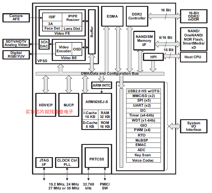
Developers can now deliver pixel-perfect images at up to 720p H.264 at 30fps in their digital video designs without concerns of video format support, constrained network bandwidth, limited system storage capacity or cost with the new TMS320DM365 digital media processor based on DaVinci technology from Texas Instruments Incorporated (TI). With multi-format HD video, the DM365 also features a suite of peripherals saving developers on system costs.
This ARM9-based DM365 device offers speeds up to 300 MHz and supports production-qualified H.264, MPEG-4, MPEG-2, MJPEG and VC1/WMV9 codecs providing customers with the flexibility to select the right video codec for their application. These codecs are driven from video accelerators offloading compression needs from the ARM core so that developers can utilize the most performance from the ARM for their application. Video surveillance designers achieve greater compression efficiency providing more storage without straining the network bandwidth. Developers of media playback and camera-driven applications, such as video doorbells, digital signage, digital video recorders, portable media players and more can ensure interoperability as well as product scalability by taking advantage of the full suite of codecs supported on the DM365.
Along with multi-format HD video, the DM365 enables seamless interface to most additional external devices required for video applications. The image sensor interface is flexible enough to support CCD, CMOS, and various other interfaces such as BT.656, BT1120. The DM365 also offers a high level of integration with HD display support including, 3 built-in 10-bit HD Analog Video Digital to Analog Converters (DACs), DDR2/mDDR, Ethernet MAC, USB 2.0, integrated audio, Host Port Interface (HPI), Analog to Digital Converter, and many more features saving developers on overall system costs as well as real estate on their circuit boards allowing for a slimmer, sleeker design.
- Highlights
- High-Performance Digital Media System-on-Chip (DMSoC)
- Up to 300-MHz ARM926EJ-S Clock Rate
- Two Video Image Co-processors (HDVICP, MJCP) Engines
- Supports a Range of Encode, Decode, and Video Quality Operations
- Video Processing Subsystem
- HW Face Detect Engine
- Resize Engine from 1/16x to 8x
- 16-Bit Parallel AFE (Analog Front-End) Interface Up to 120 MHz
- 4:2:2 (8-/16-bit) Interface
- 8-/16-bit YCC and Up to 24-Bit RGB888 Digital Output
- 3 DACs for HD Analog Video Output
- Hardware On-Screen Display (OSD)
- Capable of 720p 30fps H.264 video processingNote: 216-MHz is only capable of D1 processing
- Peripherals include EMAC, USB 2.0 OTG, DDR2/NAND, 5 SPIs, 2 UARTs, 2 MMC/SD/SDIO, Key Scan
- 8 Different Boot Modes and Configurable Power-Saving Modes
- Pin-to-pin and software compatible with DM368
- Extended temperature (-40°C - 85°C) available for 300-Mhz device
- 3.3-V and 1.8-V I/O, 1.2-V/1.35-V Core
- 338-Pin Ball Grid Array at 65nm Process Technology
- High-Performance Digital Media System-on-Chip (DMSoC)
- 216-, 270-, 300-MHz ARM926EJ-S Clock Rate
- Fully Software-Compatible With ARM9?
- ARM926EJ-S? Core
- Support for 32-Bit and 16-Bit (Thumb? Mode) Instruction Sets
- DSP Instruction Extensions and Single Cycle MAC
- ARM? Jazelle? Technology
- EmbeddedICE-RT Logic for Real-Time Debug
- ARM9 Memory Architecture
- 16K-Byte Instruction Cache
- 8K-Byte Data Cache
- 32K-Byte RAM
- 16K-Byte ROM
- Little Endian
- Two Video Image Co-processors (HDVICP, MJCP) Engines
- Support a Range of Encode and Decode Operations
- H.264, MPEG4, MPEG2, MJPEG, JPEG, WMV9/VC1
- Video Processing Subsystem
- Front End Provides:
- HW Face Detect Engine
- Hardware IPIPE for Real-Time Image Processing
- Resize Engine
- Resize Images From 1/16× to 8×
- Separate Horizontal/Vertical Control
- Two Simultaneous Output Paths
- Resize Engine
- IPIPE Interface (IPIPEIF)
- Image Sensor Interface (ISIF) and CMOS Imager Interface
- 16-Bit Parallel AFE (Analog Front End) Interface Up to 120 MHz
- Glueless Interface to Common Video Decoders
- BT.601/BT.656/BT.1120 Digital YCbCr 4:2:2 (8-/16-Bit Module
- Histogram Module
- Lens distortion correction module (LDC)
- Hardware 3A statistics collection module (H3A)
- Back End Provides:
- Hardware On-Screen Display (OSD)
- Composite NTSC/PAL video encoder output
- 8-/16-bit YCC and Up to 24-Bit RGB888 Digital Output
- 3 DACs for HD Analog Video Output
- LCD Controller
- BT.601/BT.656 Digital YCbCr 4:2:2 (8-/16-Bit) Interface
- Front End Provides:
- Analog-to-Digital Convertor (ADC)
- Power Management and Real Time Clock Subsystem (PRTCSS)
- Real Time Clock
- 16-Bit Host-Port Interface (HPI)
- 10/100 Mb/s Ethernet Media Access Controller (EMAC) - Digital Media
- IEEE 802.3 Compliant
- Supports Media Independent Interface (MII)
- Management Data I/O (MDIO) Module
- Key Scan
- Voice Codec
- External Memory Interfaces (EMIFs)
- DDR2 and mDDR SDRAM 16-bit wide EMIF With 256 MByte Address Space (1.8-V I/O)
- Asynchronous16-/8-bit Wide EMIF (AEMIF)
- Flash Memory Interfaces
- NAND (8-/16-bit Wide Data)
- 16 MB NOR Flash, SRAM
- OneNAND(16-bit Wide Data)
- Flash Memory Interfaces
- Flash Card Interfaces
- Two Multimedia Card (MMC) / Secure Digital (SD/SDIO)
- SmartMedia/xD
- Enhanced Direct-Memory-Access (EDMA) Controller (64 Independent Channels)
- USB port with Integrated 2.0 High-Speed PHY that Supports
- USB 2.0 High-Speed Device
- USB 2.0 High-Speed Host (mini-host, supporting one external device)
- USB On The Go (HS-USB OTG)
- Four 64-Bit General-Purpose Timers (each configurable as two 32-bit timers)
- One 64-Bit Watch Dog Timer
- Two UARTs (One fast UART with RTS and CTS Flow Control)
- Five Serial Port Interfaces (SPI) each with two Chip-Selects
- One Master/Slave Inter-Integrated Circuit (I2C) Bus?
- One Multi-Channel Buffered Serial Port (McBSP)
- I2S
- AC97 Audio Codec Interface
- S/PDIF via Software
- Standard Voice Codec Interface (AIC12)
- SPI Protocol (Master Mode Only)
- Direct Interface to T1/E1 Framers
- Time Division Multiplexed Mode (TDM)
- 128 Channel Mode
- Four Pulse Width Modulator (PWM) Outputs
- Four RTO (Real Time Out) Outputs
- Up to 104 General-Purpose I/O (GPIO) Pins (Multiplexed with Other Device Functions)
- Boot Modes
- On-Chip ARM ROM Bootloader (RBL) to Boot From NAND Flash, MMC/SD, UART, USB, SPI, EMAC, or HPI
- AEMIF (NOR and OneNAND)
- Configurable Power-Saving Modes
- Crystal or External Clock Input (typically 19.2 Mhz, 24 MHz, 27 Mhz or 36 MHz)
- Flexible PLL Clock Generators
- Debug Interface Support
- IEEE-1149.1 (JTAG?) Boundary-Scan-Compatible
- ETB (Embedded Trace Buffer) with 4K-Bytes Trace Buffer memory
- Device Revision ID Readable by ARM
- 338-Pin Ball Grid Array (BGA) Package (ZCE Suffix), 0.65-mm Ball Pitch
- 65nm Process Technology
- 3.3-V and 1.8-V I/O, 1.2-V/ 1.35-V Internal
- Community Reesources
- TI E2E Community
- TI Embedded Processors Wiki
Please be aware that an important notice concerning availability, standard warranty, and use in critical applications of Texas Instruments semiconductor products and disclaimers thereto appears at the end of this document. Windows is a trademark of Microsoft. All other trademarks are the property of their respective owners.
- DSP
- 0
- Operating system
- Linux
- Ethernet MAC
- 10/100
- Rating
- Catalog
- Operating temperature range (C)
- 0 to 85, -40 to 85
TMS320DM365的完整型号有:TMS320DM365ZCE21、TMS320DM365ZCE27、TMS320DM365ZCE30、TMS320DM365ZCED30、TMS320DM365ZCEF,以下是这些产品的关键参数及官网采购报价:
TMS320DM365ZCE21,工作温度:0 to 85,封装:NFBGA (ZCE)-338,包装数量MPQ:160个,MSL 等级/回流焊峰值温度:Level-3-260C-168 HR,引脚镀层/焊球材料:SNAGCU,TI官网TMS320DM365ZCE21的批量USD价格:10.155(1000+)
TMS320DM365ZCE27,工作温度:0 to 85,封装:NFBGA (ZCE)-338,包装数量MPQ:160个,MSL 等级/回流焊峰值温度:Level-3-260C-168 HR,引脚镀层/焊球材料:SNAGCU,TI官网TMS320DM365ZCE27的批量USD价格:11.678(1000+)
TMS320DM365ZCE30,工作温度:0 to 85,封装:NFBGA (ZCE)-338,包装数量MPQ:160个,MSL 等级/回流焊峰值温度:Level-3-260C-168 HR,引脚镀层/焊球材料:SNAGCU,TI官网TMS320DM365ZCE30的批量USD价格:14.217(1000+)
TMS320DM365ZCED30,工作温度:-40 to 85,封装:NFBGA (ZCE)-338,包装数量MPQ:160个,MSL 等级/回流焊峰值温度:Level-3-260C-168 HR,引脚镀层/焊球材料:SNAGCU,TI官网TMS320DM365ZCED30的批量USD价格:15.233(1000+)
TMS320DM365ZCEF,工作温度:0 to 85,封装:NFBGA (ZCE)-338,包装数量MPQ:160个,MSL 等级/回流焊峰值温度:Level-3-260C-168 HR,引脚镀层/焊球材料:SNAGCU,TI官网TMS320DM365ZCEF的批量USD价格:15.233(1000+)

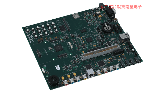
TMDXEVM368 ― TMS320DM36x 评估模块
TMS320DM36x 数字视频评估模块 (DVEVM) 使开发人员可以立即开始 DaVinci 处理器的评估,并开始构建数字视频应用,例如 IP 监控摄像机、数码相框、数字标牌、可视门铃和其它尚未发明的便携式数字视频产品。
数字视频评估模块 (DVEVM) 允许开发人员为 ARM 编写可立即投产的应用程序代码和访问使用达芬奇 API 的 HMJCP 协处理器内核,从而立即开始针对 TMS320DM365 和 TMS320DM368 数字媒体处理器的应用开发。
TMS320DM36x 数字视频评估模块 (DM36x EVM) 包含以下组件:- 基于 TMS320DM368 DaVinci (...)
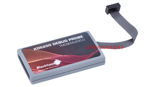
TMDSEMU200-U ― Spectrum Digital XDS200 USB 仿真器
Spectrum Digital XDS200 是最新 XDS200 系列 TI 处理器调试探针(仿真器)的首个模型。XDS200 系列拥有超低成本 XDS100 与高性能 XDS560v2 之间的低成本与高性能的完美平衡。此外,对于带有嵌入式缓冲跟踪器 (ETB) 的所有 ARM 和 DSP 处理器,所有 XDS 调试探针均支持内核和系统跟踪。
Spectrum Digital XDS200 通过 TI 20 引脚连接器(带有适合 TI 14 引脚、TI 10 引脚和 ARM 20 引脚的多个适配器)连接到目标板,而通过 USB2.0 高速连接 (480Mbps) 连接到主机 PC。要在主机 (...)
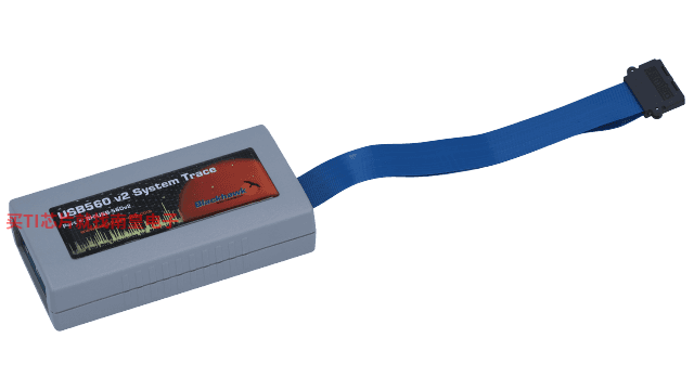
TMDSEMU560V2STM-U ― Blackhawk XDS560v2 系统跟踪 USB 仿真器
XDS560v2 System Trace 是 XDS560v2 系列高性能 TI 处理器调试探针(仿真器)的第一种型号。XDS560v2 是 XDS 系列调试探针中性能最高的一款,同时支持传统 JTAG 标准 (IEEE1149.1) 和 cJTAG (IEEE1149.7)。
XDS560v2 System Trace 在其巨大的外部存储器缓冲区中加入了系统引脚跟踪。这种外部存储器缓冲区适用于指定的 TI 器件,通过捕获相关器件级信息,获得准确的总线性能活动和吞吐量,并对内核和外设进行电源管理。此外,对于带有嵌入式缓冲跟踪器 (ETB) 的所有 ARM 和 DSP 处理器,所有 XDS (...)
TMDSEMU560V2STM-UE ― Spectrum Digital XDS560v2 系统跟踪 USB 和以太网
XDS560v2 System Trace 是 XDS560v2 系列高性能 TI 处理器调试探针(仿真器)的第一种型号。XDS560v2 是 XDS 系列调试探针中性能最高的一款,同时支持传统 JTAG 标准 (IEEE1149.1) 和 cJTAG (IEEE1149.7)。
XDS560v2 System Trace 在其巨大的外部存储器缓冲区中加入了系统引脚跟踪。这种外部存储器缓冲区适用于指定的 TI 器件,通过捕获相关器件级信息,获得准确的总线性能活动和吞吐量,并对内核和外设进行电源管理。此外,对于带有嵌入式缓冲跟踪器 (ETB) 的所有 ARM 和 DSP 处理器,所有 XDS (...)
DM365CODECS — DM36x (DM365、DM368) 编解码器 - 软件和文档
Linux 数字视频软件开发套件 (DVSDK) 使 DaVinci 系统集成商能够快速开发基于 Linux 的多媒体应用,它们可以轻松植入达芬奇平台的不同器件中。每个 DVSDK 都包含一套预先测试的操作系统、应用程序框架和具有示例程序的编解码器库,这些程序演示了从外设流入和流出的实时音频和视频数据的解码和编码。针对具有 DSP 内核的达芬奇器件,DVSDK 提供了完整的框架,便于开发人员轻松利用 DSP 加速编解码器,而无需对 DSP 进行编程。DVSDK 完全免费,无需任何运行版税。此版本 Linux DVSDK 4 版的正式 (GA) (...)
DM365 ZCE IBIS Model (Rev. C)
TI has partnered with companies to offer a wide range of software, tools, and SOMs using TI processors to accelerate your path to production. Download this search tool to quickly browse our third-party solutions and find the right third-party to meet your needs. The software, tools and modules (...)