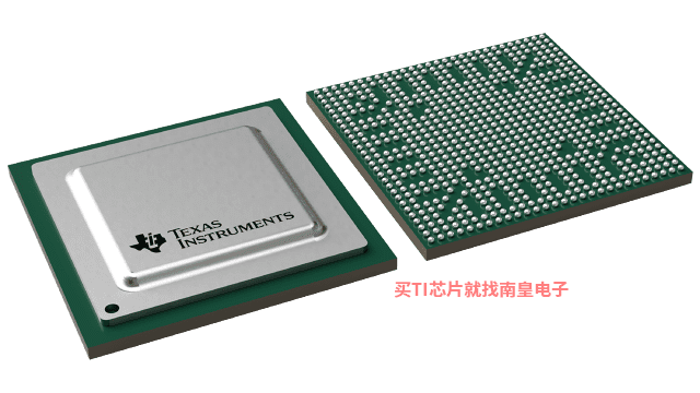
- ���쳧�̣�TI
- ��Ʒ��������� (MCU) �ʹ�����
- ������Ŀ�������� - ���� Arm �Ĵ�����
- ����������DaVinci ����ý�崦����
- ������������TMS320DM8127�ļ����ĵ�����
- TI�����������ṩ���շ������ϸ������������������Ŀ��۸�

TMS320DM8127 DaVinci Digital Media processors are highly integrated, programmable platforms that leverage the technology to meet the processing needs of the following applications to name a few:IP Network Cameras Industrial Automation Network Cameras Stereo Cameras Video Surveillance HD Video Conferencing Car Black BoxHome Audio and Video Equipment
The device enables Original-Equipment Manufacturers (OEMs) and Original-Design Manufacturers (ODMs) to quickly bring to market devices featuring robust operating systems support, rich user interfaces, and high processing performance through the maximum flexibility of a fully integrated mixed processor solution. The device also combines programmable video and audio processing with a highly integrated peripheral set.
Programmability is provided by an ARM Cortex-A8 RISC CPU with Neon extension, TI C674x VLIW floating-point DSP core, and high-definition video and imaging coprocessors. The ARM lets developers keep control functions separate from A/V algorithms programmed on the DSP and coprocessors, thus reducing the complexity of the system software. The ARM Cortex-A8 32-Bit RISC Core with Neon floating-point extension includes: 32KB of Instruction cache; 32KB of Data cache; 256KB of L2 Cache; 48KB of Boot ROM; and 64KB of RAM.
The rich peripheral set provides the ability to control external peripheral devices and communicate with external processors. For details on each of the peripherals, see the related sections in this document and the associated peripheral reference guides. The peripheral set includes: HD Video Processing Subsystem Dual Port Gigabit Ethernet MACs (10/100/1000 Mbps) [Ethernet Switch] with MII/RMII/GMII/RGMII and MDIO interface supporting IEEE 1588 Time-Stamping, AVB, and Industrial Ethernet ProtocolsTwo USB ports with integrated 2.0 PHY PCIe x1 GEN2 Compliant interfaceTwo 10-serializer McASP audio serial ports (with DIT mode)Four quad-serilaizer McASP audio serial ports (with DIT mode)One McBSP multichannel buffered serial portSix UARTs with IrDA and CIR supportFour SPI serial interfacesThree MMC/SD/SDIO serial interfacesFour I2C master and slave interfaces Parallel Camera Interface (CAM)Up to 128 General-Purpose I/Os (GPIOs)Eight 32-bit general-purpose timers System watchdog timer Dual DDR2, and DDR3 SDRAM interfacesFlexible 8- or 16-bit asynchronous memory interfaceTwo Controller Area Network (DCAN) modulesSpin LockMailbox
The TMS320DM8127 DaVinci Digital Media processors also include a high-definition video and imaging coprocessor 2 (HDVICP2) to off-load many video and imaging processing tasks from the DSP core, making more DSP MIPS available for common video and imaging algorithms. Additionally, the TMS320DM8127 DaVinci Digital Media processors have a complete set of development tools for both the ARM and DSP which include C compilers, a DSP assembly optimizer to simplify programming and scheduling, and a Microsoft? Windows? debugger interface for visibility into source code execution.
The C674x DSP core is the high-performance floating-point DSP generation in the TMS320C6000 DSP platform and is code-compatible with previous generation C64x Fixed-Point and C67x Floating-Point DSP generation. The C674x Floating-Point DSP processor uses 32KB of L1 program memory with EDC and 32KB of L1 data memory. Up to 32KB of L1P can be configured as program cache. The remaining memory is noncacheable no-wait-state program memory. Up to 32KB of L1D can be configured as data cache. The remaining memory is noncacheable no-wait-state data memory. The DSP has 256KB of L2 RAM with ECC, which can be defined as SRAM, L2 cache, or a combination of both. All C674x L3 and off-chip
- High-Performance DaVinci Video Processors
- Up to 1-GHz ARM? Cortex?-A8 RISC Core
- Up to 750-MHz C674x VLIW DSP
- Up to 6000 MIPS and 4500 MFLOPS
- Fully Software-Compatible with C67x+, C64x+
- ARM Cortex-A8 Core
- ARMv7 Architecture
- In-Order, Dual-Issue, Superscalar Processor Core
- Neon? Multimedia Architecture
- Supports Integer and Floating Point
- Jazelle? RCT Execution Environment
- ARMv7 Architecture
- ARM Cortex-A8 Memory Architecture
- 32KB of Instruction and Data Caches
- 256KB of L2 Cache
- 64KB of RAM, 48KB of Boot ROM
- TMS320C674x Floating-Point VLIW DSP
- 64 General-Purpose Registers (32-Bit)
- Six ALU (32-/40-Bit) Functional Units
- Supports 32-Bit Integer, SP (IEEE Single Precision/32-Bit) and DP (IEEE Double Precision/64-Bit) Floating Point
- Supports up to Four SP Adds Per Clock and Four DP Adds Every Two Clocks
- Supports up to Two Floating-Point (SP or DP) Approximate Reciprocal or Square Root Operations Per Cycle
- Two Multiply Functional Units
- Mixed-Precision IEEE Floating-Point Multiply Supported up to:
- 2 SP x SP �� SP Per Clock
- 2 SP x SP �� DP Every Two Clocks
- 2 SP x DP �� DP Every Three Clocks
- 2 DP x DP �� DP Every Four Clocks
- Fixed-Point Multiply Supports Two 32 x 32 Multiplies, Four 16 x 16-Bit Multiplies Including Complex Multiplies, or Eight 8 x 8-Bit Multiplies per Clock Cycle
- Mixed-Precision IEEE Floating-Point Multiply Supported up to:
- 128KB of On-Chip Memory Controller (OCMC) RAM
- Imaging Subsystem (ISS)
- Camera Sensor Connection
- Parallel Connection for Raw (up to 16-Bit) and BT.656 or BT.1120 (8- and 16-Bit)
- CSI2 Serial Connection
- Image Sensor Interface (ISIF) for Handling Image and Video Data From the Camera Sensor
- Image Pipe Interface (IPIPEIF) for Image and Video Data Connection Between Camera Sensor, ISIF, IPIPE, and DRAM
- Image Pipe (IPIPE) for Real-Time Image and Video Processing
- Resizer
- Resizing Image and Video From 1/16x to 8x
- Generating Two Different Resizing Outputs Concurrently
- Hardware 3A Engine (H3A) for Generating Key Statistics for 3A (AE, AWB, and AF) Control
- Camera Sensor Connection
- Face Detect Engine (FD)
- Hardware Face Detection for up to 35 Faces at OPP100
- Programmable High-Definition Video Image Coprocessing (HDVICP v2) Engine
- Encode, Decode, Transcode Operations
- H.264, MPEG-2, VC-1, MPEG-4, SP/ASP, JPEG/MJPEG
- Media Controller
- Controls the HDVPSS and ISS
- Endianness
- ARM and DSP Instructions/Data �C Little Endian
- HD Video Processing Subsystem (HDVPSS)
- One 165-MHz HD Video Capture Input
- One 16- or 24-Bit Input, Splittable into Dual 8-Bit SD Capture Ports
- Two 165-MHz HD Video Display Outputs
- One 16-, 24-, or 30-Bit Output and One 16- or 24-Bit Output
- Composite or S-Video Analog Output
- Macrovision? Support Available
- Digital HDMI 1.3 Transmitter With Integrated PHY
- Advanced Video Processing Features Such as Scan, Format, Rate Conversion
- Three Graphics Layers and Compositors
- One 165-MHz HD Video Capture Input
- Dual 32-Bit DDR2/DDR3 SDRAM Interfaces
- Supports up to DDR2-800 and DDR3-1066
- Up to Eight x 8 Devices Total 2GB of Total Address Space
- Dynamic Memory Manager (DMM)
- Programmable Multi-Zone Memory Mapping and Interleaving
- Enables Efficient 2D Block Accesses
- Supports Tiled Objects in 0��, 90��, 180��, or 270�� Orientation and Mirroring
- Optimizes Interlaced Accesses
- General-Purpose Memory Controller (GPMC)
- 8- or 16-Bit Multiplexed Address and Data Bus
- 512MB of Address Space Divided Among up to 8 Chip Selects
- Glueless Interface to NOR Flash, NAND Flash (BCH/Hamming Error Code Detection), SRAM and Pseudo-SRAM
- Error Locator Module (ELM) Outside of GPMC to Provide Up to 16-Bit or 512-Byte Hardware ECC for NAND
- Flexible Asynchronous Protocol Control for Interface to FPGA, CPLD, ASICs, and so Forth
- Enhanced Direct Memory Access (EDMA) Controller
- Four Transfer Controllers
- 64 Independent DMA Channels and 8 Independent QDMA Channels
- Dual Port Ethernet (10/100/1000 Mbps) With Optional Switch
- IEEE 802.3 Compliant (3.3-V I/O Only)
- MII/RMII/GMII/RGMII Media Independent Interfaces
- Management Data I/O (MDIO) Module
- Reset Isolation
- IEEE 1588 Time-Stamping, AVB, and Industrial Ethernet Protocols
- Dual USB 2.0 Ports With Integrated PHYs
- USB2.0 High- and Full-Speed Clients
- USB2.0 High-, Full-, and Low-Speed Hosts, or OTG
- Supports End Points 0�C15
- One PCI Express 2.0 Port With Integrated PHY
- Single Port With One Lane at 5.0 GT/s
- Configurable as Root Complex or Endpoint
- Eight 32-Bit General-Purpose Timers (Timer1�C8)
- One System Watchdog Timer (WDT0)
- Six Configurable UART/IrDA/CIR Modules
- UART0 With Modem Control Signals
- Supports up to 3.6864 Mbps UART0/1/2
- Supports up to 12 Mbps UART3/4/5
- SIR, MIR, FIR (4.0 MBAUD), and CIR
- Four Serial Peripheral Interfaces (SPIs) (up to 48 MHz)
- Each With Four Chip Selects
- Three MMC/SD/SDIO Serial Interfaces (up to 48 MHz)
- Three Supporting up to 1-, 4-, or 8-Bit Modes
- Four Inter-Integrated Circuit (I2C Bus) Ports
- Six Multichannel Audio Serial Ports (McASPs)
- Dual Ten Serializer Transmit and Receive Ports
- Quad Four Serializer Transmit and Receive Ports
- DIT-Capable For S/PDIF (All Ports)
- Multichannel Buffered Serial Port (McBSP)
- Transmit and Receive Clocks up to 48 MHz
- Two Clock Zones and Two Serial Data Pins
- Supports TDM, I2S, and Similar Formats
- Real-Time Clock (RTC)
- One-Time or Periodic Interrupt Generation
- Up to 128 General-Purpose I/O (GPIO) Pins
- One Spin Lock Module with up to 128 Hardware Semaphores
- One Mailbox Module with 12 Mailboxes
- On-Chip ARM ROM Bootloader (RBL)
- Power, Reset, and Clock Management
- Multiple Independent Core Power Domains
- Multiple Independent Core Voltage Domains
- Support for Three Operating Points (OPP100, OPP120, OPP166) per Voltage Domain
- Clock Enable and Disable Control for Subsystems and Peripherals
- 32KB of Embedded Trace Buffer (ETB) and 5-Pin Trace Interface for Debug
- IEEE 1149.1 (JTAG) Compatible
- 684-Pin Pb-Free BGA Package (CYE Suffix), 0.8-mm Ball Pitch With Via Channel Technology to Reduce PCB Cost
- 45-nm CMOS Technology
- Arm CPU
- 1 Arm Cortex-A8
- Arm MHz (Max.)
- 1000
- CPU
- 32-bit
- Display type
- 2 LCD
- Ethernet MAC
- 2-Port 10/100/1000
- PCIe
- 1 PCIe Gen 2
- Hardware accelerators
- Face Detect
- Rating
- Catalog
- Power supply solution
- TPS65050
- Operating temperature range (C)
- -40 to 90, 0 to 90
TMS320DM8127�������ͺ��У�TMS320DM8127SCYE0��TMS320DM8127SCYE1��TMS320DM8127SCYE2��TMS320DM8127SCYE3��TMS320DM8127SCYED0��TMS320DM8127SCYED1��TMS320DM8127SCYED2��TMS320DM8127SCYED3����������Щ��Ʒ�Ĺؼ������������ɹ����ۣ�
TMS320DM8127SCYE0�������¶ȣ�0 to 90����װ��FCBGA (CYE)-684����װ����MPQ��60����MSL �ȼ�/��������ֵ�¶ȣ�Level-4-250C-72 HR�����ŶƲ�/������ϣ�Call TI��TI����TMS320DM8127SCYE0������USD�۸�36.91��1000+��
TMS320DM8127SCYE1�������¶ȣ�0 to 90����װ��FCBGA (CYE)-684����װ����MPQ��60����MSL �ȼ�/��������ֵ�¶ȣ�Level-4-250C-72 HR�����ŶƲ�/������ϣ�Call TI��TI����TMS320DM8127SCYE1������USD�۸�39.863��1000+��
TMS320DM8127SCYE2�������¶ȣ�0 to 90����װ��FCBGA (CYE)-684����װ����MPQ��60����MSL �ȼ�/��������ֵ�¶ȣ�Level-4-250C-72 HR�����ŶƲ�/������ϣ�Call TI��TI����TMS320DM8127SCYE2������USD�۸�42.447��1000+��
TMS320DM8127SCYE3�������¶ȣ�0 to 90����װ��FCBGA (CYE)-684����װ����MPQ��60����MSL �ȼ�/��������ֵ�¶ȣ�Level-4-250C-72 HR�����ŶƲ�/������ϣ�Call TI��TI����TMS320DM8127SCYE3������USD�۸�50.567��1000+��
TMS320DM8127SCYED0�������¶ȣ�-40 to 90����װ��FCBGA (CYE)-684����װ����MPQ��60����MSL �ȼ�/��������ֵ�¶ȣ�Level-4-250C-72 HR�����ŶƲ�/������ϣ�Call TI��TI����TMS320DM8127SCYED0������USD�۸�39.494��1000+��
TMS320DM8127SCYED1�������¶ȣ�PropertyValue����װ��FCBGA (CYE)-684����װ����MPQ��60����MSL �ȼ�/��������ֵ�¶ȣ�Level-4-250C-72 HR�����ŶƲ�/������ϣ�Call TI��TI����TMS320DM8127SCYED1������USD�۸�42.447��1000+��
TMS320DM8127SCYED2�������¶ȣ�-40 to 90����װ��FCBGA (CYE)-684����װ����MPQ��60����MSL �ȼ�/��������ֵ�¶ȣ�Level-4-250C-72 HR�����ŶƲ�/������ϣ�Call TI��TI����TMS320DM8127SCYED2������USD�۸�45.03��1000+��
TMS320DM8127SCYED3�������¶ȣ�-40 to 90����װ��FCBGA (CYE)-684����װ����MPQ��60����MSL �ȼ�/��������ֵ�¶ȣ�Level-4-250C-72 HR�����ŶƲ�/������ϣ�Call TI��TI����TMS320DM8127SCYED3������USD�۸�47.614��1000+��

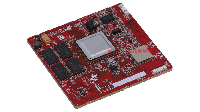
TMDSCSK8127 �� TMS320DM8127 ����������� (CSK)
���� TMS320DM8127 ����������� (CSK)��������Ա��������ʼ���� DM ����ý�崦����������ʼ��������������ӵ�������ƵӦ�á� DM8127 �ϵļ���ʽ C674x DSP ʮ���ʺ��Ӿ�����������������ǿ�ն��豸�����簲ȫ���������������¼������˶��Ϳɴ�������������˻�����Ƶ���顢���ֱ��ơ����������������������Ƶ��Ʒ����ʵʱ���ܡ�TMS320DM8127 ����������� (CSK) ����һ����װ�� I/O �ذ�� TMS320DM8127 ���������ۡ��ô����������С�� (60mm x 44mm) ��ƣ����� TMS320DM8127 ��������Դ������洢���� TI (...)
Z3-3P-VIDEO-EVMS �� Z3 ������������Ƶ����ģ��
Z3 רΪ TI �� DaVinci �� AM57x �����������˿�Դ�����ܹ����ṩ֧�֡���Ʒ�����Զ�ý��Ϊ���ĵĿ�ܡ�����������������ģ��������IJ�Ʒ��Ʒ���Z3 ��Ϊ���ߺ�����ý���Ʒ�ṩ��ϵͳ����ƺͼ��ɡ������˽��й� Z3 Technology �ĸ�����Ϣ������� http://z3technology.com�� �����ˣ� Z3 Technology
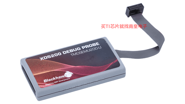
TMDSEMU200-U �� Spectrum Digital XDS200 USB ������
Spectrum Digital XDS200 ������ XDS200 ϵ�� TI ����������̽�루������������ģ�͡�XDS200 ϵ��ӵ�г��ͳɱ� XDS100 ������� XDS560v2 ֮��ĵͳɱ�������ܵ�����ƽ�⡣���⣬���ڴ���Ƕ��ʽ��������� (ETB) ������ ARM �� DSP ������������ XDS ����̽���֧���ں˺�ϵͳ���١�
Spectrum Digital XDS200 ͨ�� TI 20 �����������������ʺ� TI 14 ���š�TI 10 ���ź� ARM 20 ���ŵĶ�������������ӵ�Ŀ��壬��ͨ�� USB2.0 �������� (480Mbps) ���ӵ����� PC��Ҫ������ (...)
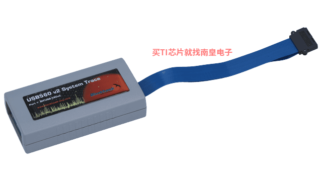
TMDSEMU560V2STM-U �� Blackhawk XDS560v2 ϵͳ���� USB ������
XDS560v2 System Trace �� XDS560v2 ϵ�и����� TI ����������̽�루���������ĵ�һ���ͺš�XDS560v2 �� XDS ϵ�е���̽����������ߵ�һ�ͬʱ֧�ִ�ͳ JTAG �� (IEEE1149.1) �� cJTAG (IEEE1149.7)��
XDS560v2 System Trace �������ⲿ�洢���������м�����ϵͳ���Ÿ��١������ⲿ�洢��������������ָ���� TI ������ͨ�����������������Ϣ�����ȷ���������ܻ���������������ں˺�������е�Դ���������⣬���ڴ���Ƕ��ʽ��������� (ETB) ������ ARM �� DSP ������������ XDS (...)
TMDSEMU560V2STM-UE �� Spectrum Digital XDS560v2 ϵͳ���� USB ����̫��
XDS560v2 System Trace �� XDS560v2 ϵ�и����� TI ����������̽�루���������ĵ�һ���ͺš�XDS560v2 �� XDS ϵ�е���̽����������ߵ�һ�ͬʱ֧�ִ�ͳ JTAG �� (IEEE1149.1) �� cJTAG (IEEE1149.7)��
XDS560v2 System Trace �������ⲿ�洢���������м�����ϵͳ���Ÿ��١������ⲿ�洢��������������ָ���� TI ������ͨ�����������������Ϣ�����ȷ���������ܻ���������������ں˺�������е�Դ���������⣬���ڴ���Ƕ��ʽ��������� (ETB) ������ ARM �� DSP ������������ XDS (...)
LINUXEZSDK-DAVINCI — ������ DM814x �� DM816x �� Linux EZ ���������� (EZSDK) - ALPHA ��
C5000/6000 Image Processing Library (IMGLIB) is an optimized image/video processing function library for C programmers. It includes C-callable general-purpose image/video processing routines that are typically used in computationally intensive real-time applications. With these routines, higher (...)SPRC265 �� TMS320C6000 DSP �� (DSPLIB)
TMS320C6000 Digital Signal Processor Library (DSPLIB) is a platform-optimized DSP function library for C programmers. It includes C-callable, general-purpose signal-processing routines that are typically used in computationally intensive real-time applications. With these routines, higher (...)DM814x, DM8127 CYE BSDL Model (Rev. A)
TI has partnered with companies to offer a wide range of software, tools, and SOMs using TI processors to accelerate your path to production. Download this search tool to quickly browse our third-party solutions and find the right third-party to meet your needs. The software, tools and modules (...)