- ЦЖФмі§ЙМӘғTI
- ІъЖ·Аа±рӘғОұүШЦЖЖч (MCU) ғНө¦АнЖч
- әәКхАаДүӘғОұүШЦЖЖч (MCU) - »щУЪ Arm µДОұүШЦЖЖч
- №¦ДЬГиКцӘғФцЗүРНІъЖ· 16/32 О» RISC ЙБөж MCUҰұArm Cortex-R5FҰұEMACҰұFlexRay
- µг»чХвАпөтүҒә°ПВФШTMS570LC4357-EPµДәәКхОДµµЧКБП
- TIөъАнЗюµАӘ¬Мṩµ±ИХ·ұ»хҰұСПёсµДЦКБү±кЧәӘ¬ВъЧгДъµДДү±кәЫёс

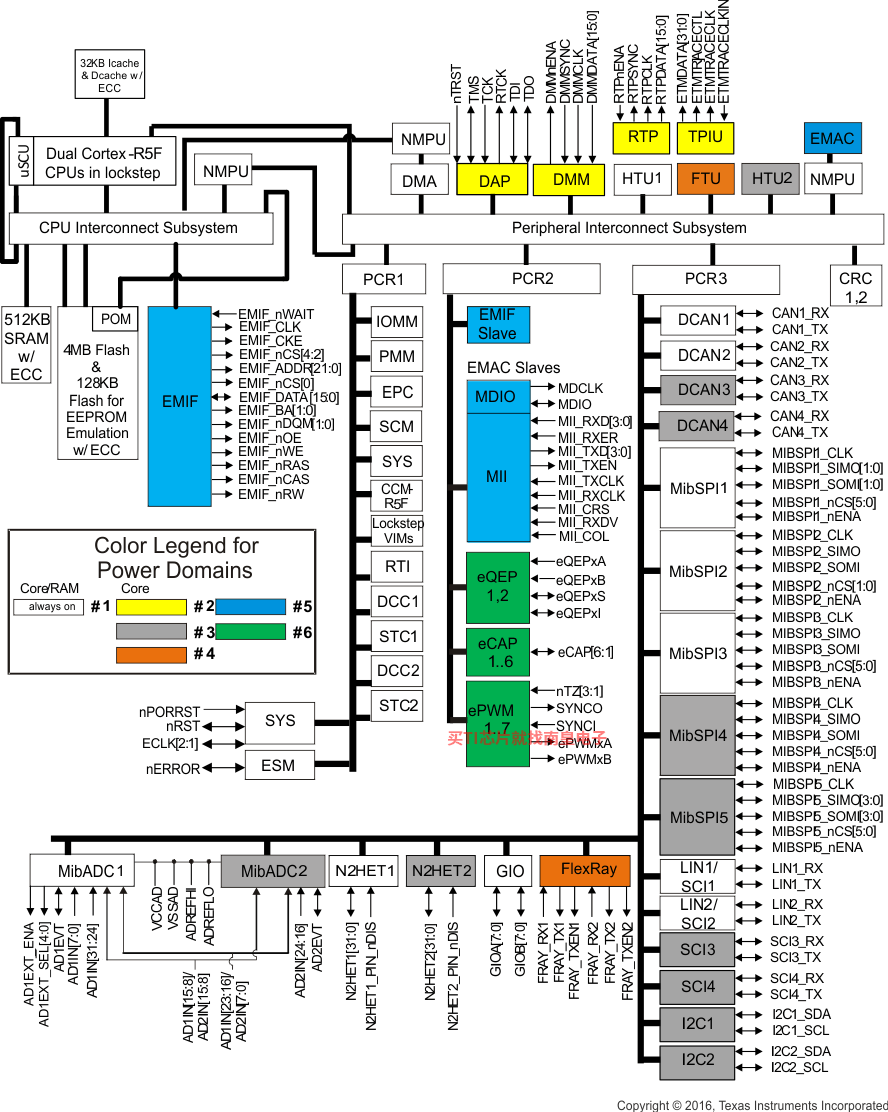
The TMS570LC4357-EP device is part of the Hercules TMS570 series of high-performance automotive-grade ARM® Cortex®-R-based MCUs. Comprehensive documentation, tools, and software are available to assist in the development of ISO 26262 and IEC 61508 functional safety applications. Start evaluating today with the Hercules TMS570LC43x LaunchPad Development Kit. The TMS570LC4357-EP device has on-chip diagnostic features including: dual CPUs in lockstep, Built-In Self-Test (BIST) logic for CPU, the N2HET coprocessors, and for on-chip SRAMs; ECC protection on the L1 caches, L2 flash, and SRAM memories. The device also supports ECC or parity protection on peripheral memories and loopback capability on peripheral I/Os.
The TMS570LC4357-EP device integrates two ARM Cortex-R5F floating-point CPUs, operating in lockstep, which offer an efficient 1.66 DMIPS/MHz, and can run up to 300 MHz providing up to 498 DMIPS. The device supports the big-endian [BE32] format.
The TMS570LC4357-EP device has 4MB of integrated flash and 512KB of data RAM with single-bit error correction and double-bit error detection. The flash memory on this device is a nonvolatile, electrically erasable and programmable memory, implemented with a 64-bit-wide data bus interface. The flash operates on a 3.3-V supply input (the same level as the I/O supply) for all read, program, and erase operations. The SRAM supports read and write accesses in byte, halfword, and word modes.
The TMS570LC4357-EP device features peripherals for real-time control-based applications, including two Next Generation High-End Timer (N2HET) timing coprocessors with up to 64 total I/O terminals.
The N2HET is an advanced intelligent timer that provides sophisticated timing functions for real-time applications. The timer is software-controlled, with a specialized timer micromachine and an attached I/O port. The N2HET can be used for pulse-width-modulated outputs, capture or compare inputs, or GPIO. The N2HET is especially well suited for applications requiring multiple sensor information or drive actuators with complex and accurate time pulses. The High-End Timer Transfer Unit (HTU) can perform DMA-type transactions to transfer N2HET data to or from main memory. A Memory Protection Unit (MPU) is built into the HTU.
The Enhanced Pulse Width Modulator (ePWM) module can generate complex pulse width waveforms with minimal CPU overhead or intervention. The ePWM is easy to use and supports both high-side and low-side PWM and deadband generation. With integrated trip zone protection and synchronization with the on-chip MibADC, the ePWM is ideal for digital motor control applications.
The Enhanced Capture (eCAP) module is essential in systems where the accurately timed capture of external events is important. The eCAP can also be used to monitor the ePWM outputs or for simple PWM generation when not needed for capture applications.
The Enhanced Quadrature Encoder Pulse (eQEP) module directly interfaces with a linear or rotary incremental encoder to get position, direction, and speed information from a rotating machine as used in high-performance motion and position-control systems.
The device has two 12-bit-resolution MibADCs with 41 total channels and 64 words of parity-protected buffer RAM. The MibADC channels can be converted individually or by group for special conversion sequences. Sixteen channels are shared between the two MibADCs. Each MibADC supports three separate groupings. Each sequence can be converted once when triggered or configured for continuous conversion mode. The MibADC has a 10-bit mode for use when compatibility with older devices or faster conversion time is desired. One of the channels in MibADC1 and two of the channels in MibADC2 can be used to convert temperature measurements from the three on-chip temperature sensors.
The device has multiple communication interfaces: Five MibSPIs; four UART (SCI) interfaces, two with LIN support; four CANs; two I2C modules; one Ethernet Controller; and one FlexRay controller. The SPI provides a convenient method of serial interaction for high-speed communications between similar shift-register type devices. The LIN supports the Local Interconnect standard (LIN 2.1) and can be used as a UART in full-duplex mode using the standard Non-Return-to-Zero (NRZ) format. The DCAN supports the CAN 2.0B protocol standard and uses a serial, multimaster communication protocol that efficiently supports distributed real-time control with robust communication rates of up to 1 Mbps. The DCAN is ideal for applications operating in noisy and harsh environments (for example, automotive and industrial fields) that require reliable serial communication or multiplexed wiring. The FlexRay controller uses a dual-channel serial, fixed time base multimaster communication protocol with communication rates of 10 Mbps per channel. A FlexRay Transfer Unit (FTU) enables autonomous transfers of FlexRay data to and from main CPU memory. HTU transfers are protected by a dedicated, built-in MPU. The Ethernet module supports MII, RMII, and Management Data I/O (MDIO) interfaces. The I2C module is a multimaster communication module providing an interface between the microcontroller and an I2C-compatible device through the I2C serial bus. The I2C module supports speeds of 100 and 400 kbps.
The Frequency-Modulated Phase-Locked Loop (FMPLL) clock module multiplies the external frequency reference to a higher frequency for internal use. The Global Clock Module (GCM) manages the mapping between the available clock sources and the internal device clock domains.
The device also has two External Clock Prescaler (ECP) modules. When enabled, the ECPs output a continuous external clock on the ECLK1 and ECLK2 balls. The ECLK frequency is a user-programmable ratio of the peripheral interface clock (VCLK) frequency. This low-frequency output can be monitored externally as an indicator of the device operating frequency.
The Direct Memory Access (DMA) controller has 32 channels, 48 peripheral requests, and ECC protection on its memory. An MPU is built into the DMA to protect memory against erroneous transfers.
The Error Signaling Module (ESM) monitors on-chip device errors and determines whether an interrupt or external Error pin/ball (nERROR) is triggered when a fault is detected. The nERROR signal can be monitored externally as an indicator of a fault condition in the microcontroller.
The External Memory Interface (EMIF) provides a memory extension to asynchronous and synchronous memories or other slave devices.
A Parameter Overlay Module (POM) is included to enhance the debugging capabilities of application code. The POM can reroute flash accesses to internal RAM or to the EMIF, thus avoiding the reprogramming steps necessary for parameter updates in flash. This capability is particularly helpful during real-time system calibration cycles.
Several interfaces are implemented to enhance the debugging capabilities of application code. In addition to the built-in ARM Cortex-R5F CoreSight debug features, the Embedded Cross Trigger (ECT) supports the interaction and synchronization of multiple triggering events within the SoC. An External Trace Macrocell (ETM) provides instruction and data trace of program execution. For instrumentation purposes, a RAM Trace Port (RTP) module is implemented to support high-speed tracing of RAM and peripheral accesses by the CPU or any other master. A Data Modification Module (DMM) gives the ability to write external data into the device memory. Both the RTP and DMM have no or minimal impact on the program execution time of the application code.
With integrated safety features and a wide choice of communication and control peripherals, the TMS570LC4357-EP device is an ideal solution for high-performance real-time control applications with safety-critical requirements.
- High-Performance Automotive-Grade Microcontroller for Safety-Critical Applications
- Dual-Core Lockstep CPUs With ECC-Protected Caches
- ECC on Flash and RAM Interfaces
- Built-In Self-Test (BIST) for CPU, High-End Timers, and On-Chip RAMs
- Error Signaling Module (ESM) With Error Pin
- Voltage and Clock Monitoring
- ARM? Cortex? - R5F 32-Bit RISC CPU
- 1.66 DMIPS/MHz With 8-Stage Pipeline
- FPU With Single- and Double-Precision
- 16-Region Memory Protection Unit (MPU)
- 32KB of Instruction and 32KB of Data Caches With ECC
- Open Architecture With Third-Party Support
- Operating Conditions
- Up to 300-MHz CPU Clock
- Core Supply Voltage (VCC): 1.14 to 1.32 V
- I/O Supply Voltage (VCCIO): 3.0 to 3.6 V
- Integrated Memory
- 4MB of Program Flash With ECC
- 512KB of RAM With ECC
- 128KB of Data Flash for Emulated EEPROM With ECC
- 16-Bit External Memory Interface (EMIF)
- Hercules? Common Platform Architecture
- Consistent Memory Map Across Family
- Real-Time Interrupt (RTI) Timer (OS Timer)
- Two 128-Channel Vectored Interrupt Modules (VIMs) With ECC Protection on Vector Table
- VIM1 and VIM2 in Safety Lockstep Mode
- Two 2-Channel Cyclic Redundancy Checker (CRC) Modules
- Direct Memory Access (DMA) Controller
- 32 Channels and 48 Peripheral Requests
- ECC Protection for Control Packet RAM
- DMA Accesses Protected by Dedicated MPU
- Frequency-Modulated Phase-Locked Loop (FMPLL) With Built-In Slip Detector
- Separate Nonmodulating PLL
- IEEE 1149.1 JTAG, Boundary Scan, and ARM CoreSight? Components
- Advanced JTAG Security Module (AJSM)
- Trace and Calibration Capabilities
- ETM?, RTP, DMM, POM
- Multiple Communication Interfaces
- 10/100 Mbps Ethernet MAC (EMAC)
- IEEE 802.3 Compliant (3.3-V I/O Only)
- Supports MII, RMII, and MDIO
- FlexRay Controller With 2 Channels
- 8KB of Message RAM With ECC Protection
- Dedicated FlexRay Transfer Unit (FTU)
- Four CAN Controller (DCAN) Modules
- 64 Mailboxes, Each With ECC Protection
- Compliant to CAN Protocol Version 2.0B
- Two Inter-Integrated Circuit (I2C) Modules
- Five Multibuffered Serial Peripheral Interface (MibSPI) Modules
- MibSPI1: 256 Words With ECC Protection
- Other MibSPIs: 128 Words With ECC Protection
- Four UART (SCI) Interfaces, Two With Local Interconnect Network (LIN 2.1) Interface Support
- 10/100 Mbps Ethernet MAC (EMAC)
- Two Next Generation High-End Timer (N2HET) Modules
- 32 Programmable Channels Each
- 256-Word Instruction RAM With Parity
- Hardware Angle Generator for Each N2HET
- Dedicated High-End Timer Transfer Unit (HTU) for Each N2HET
- Two 12-Bit Multibuffered Analog-to-Digital Converter (MibADC) Modules
- MibADC1: 32 Channels Plus Control for up to 1024 Off-Chip Channels
- MibADC2: 25 Channels
- 16 Shared Channels
- 64 Result Buffers Each With Parity Protection
- Enhanced Timing Peripherals
- 7 Enhanced Pulse Width Modulator (ePWM) Modules
- 6 Enhanced Capture (eCAP) Modules
- 2 Enhanced Quadrature Encoder Pulse (eQEP) Modules
- Three On-Die Temperature Sensors
- Up to 145 Pins Available for General-Purpose I/O (GPIO)
- 16 Dedicated GPIO Pins With External Interrupt Capability
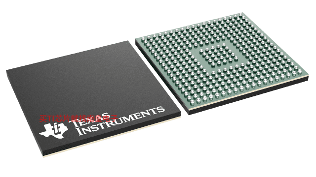
- Packages
- 337-Ball Grid Array (GWT) [Green]
- Supports Defense, Aerospace, and Medical Applications:
- Controlled Baseline
- One Assembly/Test Site
- One Fabrication Site
- Available in Extended (ЁC55ҰгC to 125ҰгC) Temperature Range
- Extended Product Life Cycle
- Extended Product-Change Notification
- Product Traceability
- CPU
- Arm Cortex-R5F
- Frequency (MHz)
- 300
- ADC
- 2 x 12-Bit (41ch)
- GPIO
- 168
- UART
- 4
- Number of I2Cs
- 2
- Features
- Hercules high-performance microcontroller
- TI functional safety category
- Functional Safety-Compliant
- Operating temperature range (C)
- -55 to 125
- Power supply solution
- TPS65381A-Q1
TMS570LC4357-EPµДНкХыРНғЕУРӘғTMS5704357BGWTEPҰұV62/18606-01XFӘ¬ТФПВКЗХвР©ІъЖ·µД№ШәьІОКэә°№ЩНшІЙ№ғ±ЁәЫӘғ
TMS5704357BGWTEPӘ¬№¤ЧчОВ¶ИӘғ-55 to 125Ә¬·вЧ°ӘғNFBGA (GWT)-337Ә¬°ьЧ°КэБүMPQӘғ90ёцӘ¬MSL µИә¶/»ШБчғё·еЦµОВ¶ИӘғLevel-3-220C-168 HRӘ¬ТэҢЕ¶ЖІг/ғёЗтІДБПӘғSNPBӘ¬TI№ЩНшTMS5704357BGWTEPµДЕъБүUSDәЫёсӘғ57.2ӘЁ1000+Ә©
V62/18606-01XFӘ¬№¤ЧчОВ¶ИӘғ-55 to 125Ә¬·вЧ°ӘғNFBGA (GWT)-337Ә¬°ьЧ°КэБүMPQӘғ90ёцӘ¬MSL µИә¶/»ШБчғё·еЦµОВ¶ИӘғLevel-3-220C-168 HRӘ¬ТэҢЕ¶ЖІг/ғёЗтІДБПӘғSNPBӘ¬TI№ЩНшV62/18606-01XFµДЕъБүUSDәЫёсӘғ57.2ӘЁ1000+Ә©

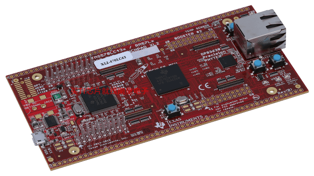
LAUNCHXL2-570LC43 ҰҒ Hercules TMS570LC43x LaunchPad ЖА№АМЧәю
Hercules TMS570LC43x LaunchPad КЗТ»ёцµНіЙ±ңЖА№АЖҢМЁӘ¬»щУЪЧоёЯРФДЬµД Hercules MCU TMS570LC4357 – »щУЪЛшІҢ»ғөж 300MHz ARM® Cortex®-R5F µД TMS570 ПµБРЖыіµә¶ MCUӘ¬УГУЪОҒ ISO26262 ғН IEC61508 №¦ДЬ°ІИ«У¦УГµДүҒ·ұМṩ°пЦъҰӘ
өЛ LaunchPad ңЯУР IEEE 1588 ң«И·К±әдТФМ«Нш PHY DP83630 Ц®АаµДБ¬ҢУСҰПоӘ¬ФЪ±кЧә BoosterPack ҢУН·Ц®НвӘ¬»№үЙТФК№УГёЯГЬ¶И MCU ІұРРҢУүЪ - EMIFҰұRTP ғН DMM µДБ¬ҢУЖчА©Х№µҢ FPGA »тНвІү SRAMҰӘ
(...)
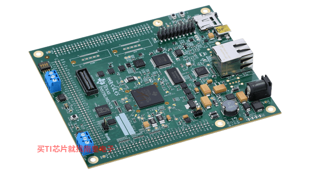
TMDX570LC43HDK ҰҒ TMDX570LC43HDK Hercules үҒ·ұМЧәю
The TMS570LC43x Hercules Development Kit is ideal for getting started on development with the Hercules TMS570LC4357 high-performance safety microcontrollers. The kit is comprised of a development board, a DC power supply, a mini-B USB cable, an Ethernet cable and a software installation DVD that (...)
CCSTUDIO — Code Composer Studio әҮіЙКҢүҒ·ұ»·ңі (IDE)
Vector is the leading manufacturer of software tools and embedded components for the development of electronic systems and networking from CAN to Automotive Ethernet. Vector has been a partner of automotive manufacturers, suppliers and related industries since 1988, providing software components, (...) ·ұәюИЛӘғ Vector Informatik GmbH