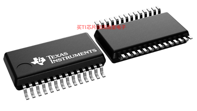
- 制造厂商:TI
- 产品类别:电源管理
- 技术类目:栅极驱动器 - 低侧驱动器
- 功能描述:1.2mA/1.2mA 6 通道栅极驱动器,可在负载短路、负载开路和电池过压时转换至低占空比 PWM
- 点击这里打开及下载TPIC46L02的技术文档资料
- TI代理渠道,提供当日发货、严格的质量标准,满足您的目标价格

The TPIC46L01, TPIC46L02, and TPIC46L03 are low-side predrivers that provide serial input interface and parallel input interface to control six external field-effect transistor(FET) power switches such as offered in the Texas Instruments TPIC family of power arrays. These devices are designed primarily for low-frequency switching, inductive load applications such as solenoids and relays. Fault status for each channel is available in a serial-data format. Each driver channel has independent off-state open-load detection and on-state shorted-load/short-to-battery detection. Battery overvoltage and undervoltage detection and shutdown are provided. Battery and output load faults provide real-time fault reporting to the controller. Each channel also provides inductive-voltage-transient protection for the external FET.
These devices provide control of output channels through a serial input interface or a parallel input interface. A command to enable the output from either interface enables the respective channel GATE output to the external FET. The serial input interface is recommended when the number of signals between the control device and the predriver must be minimized, and the speed of operation is not critical. In applications where the predriver must respond very quickly or asynchronously, the parallel input interface is recommended.
For serial operation, the control device must transition CS\ from high to low to activate the serial input interface. When this occurs, SDO is enabled, fault data is latched into the serial input interface, and the FLT\ flag is refreshed.
Data is clocked into the serial registers on low-to-high transitions of SCLK through SDI. Each string of data must consist of 8 bits of data. In applications where multiple devices are cascaded together, the string of data must consist of 8 bits for each device. A high data bit turns the respective output channel on and a low data bit turns it off. Fault data for the device is clocked out of SDO as serial input data is clocked into the device. Fault data consists of fault flags for the over-battery voltage (bit 8), under-battery voltage (bit 7) (not on TPIC46L03), and shorted/open-load flags (bits 1-6) for each of the six output channels. A logic-high bit in the fault data indicates a fault and a logic-low bit indicates that no fault is present on that channel. Fault register bits are set or cleared asynchronously to reflect the current state of the hardware. The fault must be present when CS\ is transitioned from high to low to be captured and reported in the serial fault data. New faults cannot be captured in the serial register when CS\ is low. CS\ must be transitioned high after all of the serial data has been clocked into the device. A low-to-high transition of CS\ transfers the last 6 bits of serial data to the output buffer, puts SDO in a high-impedance state, and clears and reenables the fault register. The TPIC46L01/L02/L03 was designed to allow the serial input interfaces of multiple devices to be cascaded together to simplify the serial interface to the controller. Serial input data flows through the device and is transferred out SDO following the fault data in cascaded configurations.
For parallel operation, data is asynchronously transferred directly from the parallel input interface (IN0-IN5) to the respective GATE output. SCLK or CS\ are not required for parallel control. A 1 on the parallel input turns the respective channel on, where a 0 turns it off. Note that either the serial interface or the parallel interface can enable a channel. Under parallel operation, fault data must still be collected through the serial data interface.
The predrivers monitor the drain voltage for each channel to detect shorted-load or open-load fault conditions in the on and off states respectively. These devices offer the option of using an internally generated fault-reference voltage or an externally supplied VCOMP for fault detection. The internal fault reference is selected by connecting VCOMPEN to GND and the external reference is selected by connecting VCOMPEN to VCC. The drain voltage is compared to the fault-reference voltage when the channel is turned on to detect shorted-load conditions and when the channel is off to detect open-load conditions. When a shorted-load fault occurs using the TPIC46L01 or TPIC46L03, the channel is turned off and a fault signal is sent to FLT\ as well as to the serial fault-register bit. When a shorted-load fault occurs while using the TPIC46L02, the channel transitions into a low-duty cycle, pulse-width-modulated (PWM) signal as long as the fault is present. Shorted-load conditions must be present for at least the shorted-load deglitch time, t(STBDG), in order to be flagged as a fault. A fault signal is sent to FLT\ as well as the serial fault register bit. More detail on fault detection operation is presented in the device operation section of this data sheet.
The TPIC46L01 and TPIC46L02 provide protection from over-battery voltage and under-battery voltage conditions irrespective of the state of the output channels. The TPIC46L03 provides protection from over-battery voltage conditions irrespective of the state of the output channels When the battery voltage is greater than the overvoltage threshold or less than the undervoltage threshold (except for the TPIC46L03, which has no undervoltage threshold), all channels are disabled and a fault signal is sent to FLT\ as well as to the respective fault register bits. The outputs return to normal operation once the battery voltage fault has been corrected. When an over-battery/under-battery voltage condition occurs, the device reports the battery fault, but disables fault reporting for open and shorted-load conditions. Fault reporting for open and shorted-load conditions are reenabled after the battery fault condition has been corrected.
These devices provide inductive transient protection on all channels. The drain voltage is clamped to protect the FET. This clamp voltage is defined by the sum of VCC and turn-on voltage of the external FET. The predriver also provides a gate-to-source voltage (VGS) clamp to protect the GATE-source terminals of the power FET from exceeding their rated voltages.
These devices provide pulldown resistors on all inputs except CS\. A pullup resistor is used on CS\.
- 6-Channel Serial-In/Parallel-In Low-side Pre-FET Driver
- Device Can Be Cascaded
- Internal 55-V Inductive Load Clamp and VGS Protection Clamp for External Power FETs
- Independent Shorted-Load/Short-to-Battery Fault Detection on All Drain Terminals
- Independent Off-State Open-Load Fault Sense
- Over-Battery-Voltage Lockout Protection and Fault Reporting
- Under-Battery Voltage Lockout Protection for TPIC46L01 and TPIC46L02
- Asynchronous Open-Drain Fault Flag
- Device Output Can Be Wire-ORed With Multiple External Devices
- Fault Status Returned Through Serial Output Terminal
- Internal Global Power-On Reset of Device
- High-Impedance CMOS Compatible Inputs With Hysteresis
- TPIC46L01 and TPIC46L03 Disables the Gate Output When a Shorted-Load Fault Occurs
- TPIC46L02 Transitions the Gate Output to a Low-Duty Cycle PWM Mode When a Shorted-Load Fault Occurs
- Number of channels (#)
- 6
- Power switch
- MOSFET
- Peak output current (A)
- 0.0012
- Input VCC (Min) (V)
- 8
- Input VCC (Max) (V)
- 24
- Features
- SPI Interface, Sleep Mode, OVP, Fault Diagnostics
- Operating temperature range (C)
- -40 to 125
- Rise time (ns)
- 3500
- Fall time (ns)
- 3000
- Prop delay (ns)
- 5000
- Input threshold
- CMOS
- Channel input logic
- Non-Inverting
- Input negative voltage (V)
- -0.3
- Rating
- Automotive
- Driver configuration
- Hex
TPIC46L02的完整型号有:TPIC46L02DB、TPIC46L02DBG4、TPIC46L02DBR、TPIC46L02DBRG4,以下是这些产品的关键参数及官网采购报价:
TPIC46L02DB,工作温度:-40 to 125,封装:SSOP (DB)-28,包装数量MPQ:50个,MSL 等级/回流焊峰值温度:Level-1-260C-UNLIM,引脚镀层/焊球材料:NIPDAU,TI官网TPIC46L02DB的批量USD价格:1.214(1000+)
TPIC46L02DBG4,工作温度:PropertyValue,封装:SSOP (DB)-28,包装数量MPQ:50个,MSL 等级/回流焊峰值温度:Level-1-260C-UNLIM,引脚镀层/焊球材料:NIPDAU,TI官网TPIC46L02DBG4的批量USD价格:1.366(1000+)
TPIC46L02DBR,工作温度:-40 to 125,封装:SSOP (DB)-28,包装数量MPQ:2000个,MSL 等级/回流焊峰值温度:Level-1-260C-UNLIM,引脚镀层/焊球材料:NIPDAU,TI官网TPIC46L02DBR的批量USD价格:1.012(1000+)
TPIC46L02DBRG4,工作温度:-40 to 125,封装:SSOP (DB)-28,包装数量MPQ:2000个,MSL 等级/回流焊峰值温度:Level-1-260C-UNLIM,引脚镀层/焊球材料:NIPDAU,TI官网TPIC46L02DBRG4的批量USD价格:1.164(1000+)

TPIC46L02 TINA-TI Transient Spice Model
PSpice for TI 可提供帮助评估模拟电路功能的设计和仿真环境。此功能齐全的设计和仿真套件使用 Cadence 的模拟分析引擎。PSpice for TI 可免费使用,包括业内超大的模型库之一,涵盖我们的模拟和电源产品系列以及精选的模拟行为模型。借助?PSpice for TI 的设计和仿真环境及其内置的模型库,您可对复杂的混合信号设计进行仿真。创建完整的终端设备设计和原型解决方案,然后再进行布局和制造,可缩短产品上市时间并降低开发成本。
在?PSpice for TI 设计和仿真工具中,您可以搜索 TI (...)


