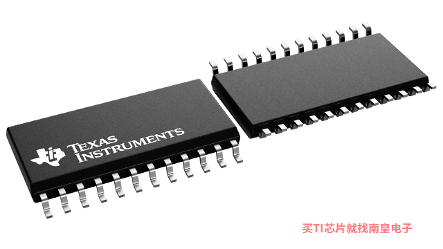
- 制造厂商:TI
- 产品类别:电源管理
- 技术类目:LED 驱动器 - 汽车 LED 驱动器
- 功能描述:用于增强级联、具有使能/关断功能的 8 位移位寄存器
- 点击这里打开及下载TPIC6A596的技术文档资料
- TI代理渠道,提供当日发货、严格的质量标准,满足您的目标价格

The TPIC6A596 is a monolithic, high-voltage, high-current power logic 8-bit shift register designed for use in systems that require relatively high load power. The device contains a built-in voltage clamp on the outputs for inductive transient protection. Power driver applications include relays, solenoids, and other medium-current or high-voltage loads. Each open-drain DMOS transistor features an independent chopping current-limiting circuit to prevent damage in the case of a short circuit.
This device contains an 8-bit serial-in, parallel-out shift register that feeds an 8-bit, D-type storage register. Data transfers through both the shift and storage registers on the rising edge of the shift-register clock (SRCK) and the register clock (RCK), respectively. The storage register transfers data to the output buffer when shift-register clear (SRCLR)\ is high. When SRCLR\ is low, all registers in the device are cleared. When output enable G\ is held high, all data in the output buffers is held low and all drain outputs are off. When G\ is held low, data from the storage register is transparent to the output buffers. The serial output (SER OUT) is clocked out of the device on the falling edge of SRCK to provide additional hold time for cascaded applications. This will provide improved performance for applications where clock signals may be skewed, devices are not located near one another, or the system must tolerate electromagnetic interference.
Outputs are low-side, open-drain DMOS transistors with output ratings of 50 V and a 350-mA continuous sink current capability. When data in the output buffers is low, the DMOS-transistor outputs are off. When data is high, the DMOS-transistor outputs have sink current capability.
Separate power ground (PGND) and logic ground (LGND) terminals are provided to facilitate maximum system flexibility. All PGND terminals are internally connected, and each PGND terminal must be externally connected to the power system ground in order to minimize parasitic impedance. A single-point connection between LGND and PGND must be made externally in a manner that reduces crosstalk between the logic and load circuits.
The TPIC6A596 is offered in a thermally-enhanced dual-in-line (NE) package and a wide-body surface-mount (DW) package. The TPIC6A596 is characterized for operation over the operating case temperature range of -40°C to 125°C.
- Low rDS(on) . . . 1 Typ
- Output Short-Circuit Protection
- Avalanche Energy . . . 75 mJ
- Eight 350-mA DMOS Outputs
- 50-V Switching Capability
- Enhanced Cascading for Multiple Stages
- All Registers Cleared With Single Input
- Low Power Consumption
- Number of channels (#)
- 8
- Topology
- Open drain
- Rating
- Automotive
- Operating temperature range (C)
- -40 to 125
- Vin (Min) (V)
- 4.5
- Vin (Max) (V)
- 5.5
- Vout (Max) (V)
- 50
- Features
- Enable/Shutdown, Thermal Shutdown
TPIC6A596的完整型号有:TPIC6A596DW、TPIC6A596DWG4、TPIC6A596DWRG4、TPIC6A596NE,以下是这些产品的关键参数及官网采购报价:
TPIC6A596DW,工作温度:-40 to 125,封装:SOIC (DW)-24,包装数量MPQ:25个,MSL 等级/回流焊峰值温度:Level-1-260C-UNLIM,引脚镀层/焊球材料:NIPDAU,TI官网TPIC6A596DW的批量USD价格:1.38(1000+)
TPIC6A596DWG4,工作温度:-40 to 125,封装:SOIC (DW)-24,包装数量MPQ:25个,MSL 等级/回流焊峰值温度:Level-1-260C-UNLIM,引脚镀层/焊球材料:NIPDAU,TI官网TPIC6A596DWG4的批量USD价格:1.553(1000+)
TPIC6A596DWRG4,工作温度:-40 to 125,封装:SOIC (DW)-24,包装数量MPQ:2000个,MSL 等级/回流焊峰值温度:Level-1-260C-UNLIM,引脚镀层/焊球材料:NIPDAU,TI官网TPIC6A596DWRG4的批量USD价格:1.323(1000+)
TPIC6A596NE,工作温度:-40 to 125,封装:PDIP (NE)-20,包装数量MPQ:20个,MSL 等级/回流焊峰值温度:N/A for Pkg Type,引脚镀层/焊球材料:NIPDAU,TI官网TPIC6A596NE的批量USD价格:1.553(1000+)

PSPICE-FOR-TI — 适用于 TI 设计和模拟工具的 PSpice
PSpice for TI 可提供帮助评估模拟电路功能的设计和仿真环境。此功能齐全的设计和仿真套件使用 Cadence 的模拟分析引擎。PSpice for TI 可免费使用,包括业内超大的模型库之一,涵盖我们的模拟和电源产品系列以及精选的模拟行为模型。借助?PSpice for TI 的设计和仿真环境及其内置的模型库,您可对复杂的混合信号设计进行仿真。创建完整的终端设备设计和原型解决方案,然后再进行布局和制造,可缩短产品上市时间并降低开发成本。
在?PSpice for TI 设计和仿真工具中,您可以搜索 TI (...)


