- 制造厂商:TI
- 产品类别:电源管理
- 技术类目:监控器和复位 IC
- 功能描述:适用于开关模式电源、具有过流检测功能的 3 通道监控器
- 点击这里打开及下载TPS3513的技术文档资料
- TI代理渠道,提供当日发货、严格的质量标准,满足您的目标价格

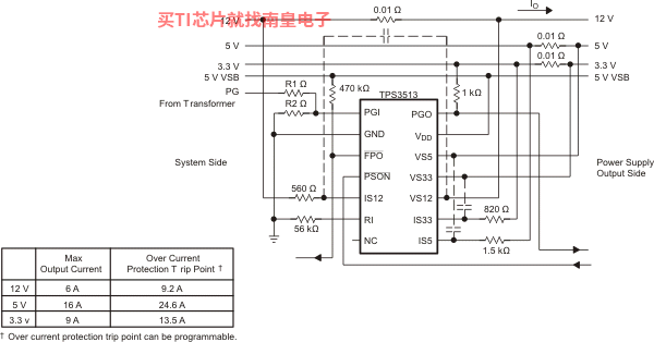
The TPS3513 is designed to optimize PC switching power supply system with minimum external components. It provides undervoltage lockout (UVLO), protection circuits, power good indicator, and on/off control.
UVLO thresholds are 4.45 V (on) and 3.65 V (off). Overcurrent protection (OCP) and overvoltage protection (OVP) monitor 3.3 V, 5 V, and 12 V. When an OC or OV condition is detected, the power-good output (PGO) is asserted low and the fault protection output (FPO) is latched high. PSON from low-to-high resets the latch. The OCP function will be enabled 75 ms after PSON goes low, and a debounce of typically 38 ms. A built-in 2.3-ms delay with 38-ms debounce from PSON to FPO output is enabled at turnoff.
An external resistor is connected between the RI pin and the GND pin. This will introduce an accurate I(ref) for OCP function. The I(ref) range is from 12.5 µA to 62.5 µA. The formula for choosing RI resistor is V(RI)/I(ref). Three OCP comparators and the I(ref) section are supplied by VS12. The current draw from the VS12 pin is less than 1 mA.
The power good feature monitors PGI, 3.3 V and 5 V, and issues a power good signal when the output is ready.
The TPS3513 is characterized for operation from –40°C to 85°C.
- Overvoltage Protection and Lockout for 12?V, 5 V, and 3.3 V
- Overcurrent Protection and Lockout for 12 V, 5 V, and 3.3 V
- Undervoltage Protection and Lockout for?12 V, and Undervoltage Detect for 5 V and 3.3 V
- Fault-Protection Output With Open Drain Output Stage
- Open-Drain, Power Good Output Signal for Power-Good Input, 3.3 V and 5 V
- 300-ms Power-Good Delay
- 75-ms Delay for 5-V and 3.3-V Power Supply Short-Circuit Turnon Protection
- 2.3 ms PSON Control to FPO Turnoff Delay
- 38 ms PSON Control Debounce
- Wide Supply Voltage Range From 4.5 V to?15 V
- Number of supplies monitored
- 3
- Threshold voltage 1 (Typ) (V)
- 2.2
- Features
- Overcurrent sense, Undervoltage and overvoltage monitor, PFI/PFO, Wide input voltage
- Reset threshold accuracy (%)
- 2.3
- Output driver type/reset output
- Active-low, Open-drain
- Time delay (ms)
- 300
- Rating
- Catalog
- Watchdog timer WDI (sec)
- None
- Operating temperature range (C)
- -40 to 85
TPS3513的完整型号有:TPS3513D、TPS3513DR、TPS3513N,以下是这些产品的关键参数及官网采购报价:
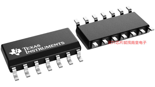
TPS3513D,工作温度:-40 to 85,封装:SOIC (D)-14,包装数量MPQ:50个,MSL 等级/回流焊峰值温度:Level-1-260C-UNLIM,引脚镀层/焊球材料:NIPDAU,TI官网TPS3513D的批量USD价格:1.355(1000+)
TPS3513DR,工作温度:-40 to 85,封装:SOIC (D)-14,包装数量MPQ:2500个,MSL 等级/回流焊峰值温度:Level-1-260C-UNLIM,引脚镀层/焊球材料:NIPDAU,TI官网TPS3513DR的批量USD价格:1.138(1000+)
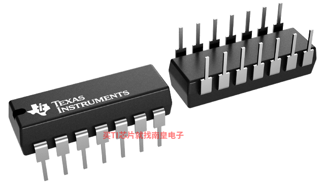
TPS3513N,工作温度:-40 to 85,封装:PDIP (N)-14,包装数量MPQ:25个,MSL 等级/回流焊峰值温度:N/A for Pkg Type,引脚镀层/焊球材料:NIPDAU,TI官网TPS3513N的批量USD价格:1.301(1000+)

PSPICE-FOR-TI ― 适用于 TI 设计和模拟工具的 PSpice
PSpice for TI 可提供帮助评估模拟电路功能的设计和仿真环境。此功能齐全的设计和仿真套件使用 Cadence 的模拟分析引擎。PSpice for TI 可免费使用,包括业内超大的模型库之一,涵盖我们的模拟和电源产品系列以及精选的模拟行为模型。借助?PSpice for TI 的设计和仿真环境及其内置的模型库,您可对复杂的混合信号设计进行仿真。创建完整的终端设备设计和原型解决方案,然后再进行布局和制造,可缩短产品上市时间并降低开发成本。
在?PSpice for TI 设计和仿真工具中,您可以搜索 TI (...)
