- 制造厂商:TI
- 产品类别:电源管理
- 技术类目:直流/直流开关稳压器 - 降压稳压器
- 功能描述:适用于 VR13 CPU VCORE 和 DDR 存储器的两相 D-CAP+ 降压控制器
- 点击这里打开及下载TPS53626的技术文档资料
- TI代理渠道,提供当日发货、严格的质量标准,满足您的目标价格

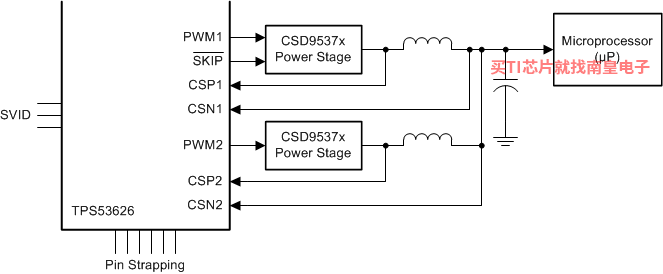
The TPS53626 device is a driverless, VR13 SVID compliant, synchronous buck controller.Advanced control features such as D-CAP+ architecture with overlapping pulse support undershoot reduction (USR) and overshoot reduction (OSR) provide fasttransient response, lowest output capacitance and high efficiency. The device also supportssingle-phase operation in CCM or DCM for light-load efficiency boost. The device integrates a fullset of VR13 I/O features including VR_READY (PGOOD), ALERT and VR_HOT. The SVID interface address allows programming from 00h to 07h.Adjustable control of VOUT slew rate can be programmed as high as20mV/uS.
Paired with the TI NexFET Power Stage, this totalsolution delivers exceptionally high speed and low switching loss. The TPS53626 also offers four default modes that configure VCCIO and VMCP settings with one single external resistor to savecomponent count and board space.
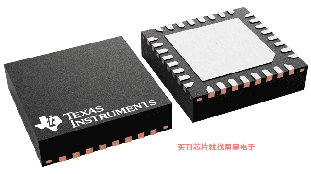
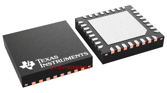
The TPS53626 device package is a space saving, thermally enhanced 32-pin VQFN packagethat operates from –40°C to 105°C.
For all available packages, see the orderable addendum at the end of the document.- Intel VR13 Serial VID (SVID) Compliant
- 1- or 2-Phase Operation
- Default Configuration Mode for VR13 VCCIO and VMCP
- Supports Both Droop and Non-Droop Applications
- 8-Bit DAC with 5-mV Step
- Output Range: 0.25 V to 1.52 V
- Optimized Efficiency at Light and Heavy Loads
- 8 Independent Levels of Overshoot Reduction (OSR) and Undershoot Reduction (USR)
- Driverless Configuration for Efficient High-Frequency Switching
- Supports Discrete, Power Block, Power Stage or DrMOS MOSFET Implementations
- Accurate, Adjustable Voltage Positioning
- 300-kHz to 1-MHz Frequency Selections
- Patented AutoBalance Phase Balancing
- Programmable ON-Pulse Extension for Load Transient Boost
- Programmable Auto DCM and CCM Operation
- Selectable 8-level Current Limit
- 4.5-V to 28-V Conversion Voltage Range
- Small, 4 mm × 4 mm, 32-Pin, VQFN PowerPad Package
- Vin (Min) (V)
- 4.5
- Vin (Max) (V)
- 28
- Vout (Min) (V)
- 0.25
- Vout (Max) (V)
- 1.52
- Iout (Max) (A)
- 70
- Iq (Typ) (uA)
- 3500
- Switching frequency (Min) (kHz)
- 300
- Switching frequency (Max) (kHz)
- 1000
- Features
- Adjustable Current Limit, Dynamic Voltage Scaling, Enable, Light Load Efficiency, Output Discharge, Phase Interleaving, Power Good, Pre-Bias Start-Up, Remote Sense, SVID, Synchronous Rectification
- Regulated outputs (#)
- 1
- Number of phases
- 2
- Rating
- Catalog
TPS53626的完整型号有:TPS53626RSMR、TPS53626RSMT,以下是这些产品的关键参数及官网采购报价:
TPS53626RSMR,工作温度:-40 to 105,封装:VQFN (RSM)-32,包装数量MPQ:3000个,MSL 等级/回流焊峰值温度:Level-2-260C-1 YEAR,引脚镀层/焊球材料:NIPDAU,TI官网TPS53626RSMR的批量USD价格:2.081(1000+)
TPS53626RSMT,工作温度:-40 to 105,封装:VQFN (RSM)-32,包装数量MPQ:250个,MSL 等级/回流焊峰值温度:Level-2-260C-1 YEAR,引脚镀层/焊球材料:NIPDAU,TI官网TPS53626RSMT的批量USD价格:2.497(1000+)

PSPICE-FOR-TI — 适用于 TI 设计和模拟工具的 PSpice
PSpice for TI 可提供帮助评估模拟电路功能的设计和仿真环境。此功能齐全的设计和仿真套件使用 Cadence 的模拟分析引擎。PSpice for TI 可免费使用,包括业内超大的模型库之一,涵盖我们的模拟和电源产品系列以及精选的模拟行为模型。借助?PSpice for TI 的设计和仿真环境及其内置的模型库,您可对复杂的混合信号设计进行仿真。创建完整的终端设备设计和原型解决方案,然后再进行布局和制造,可缩短产品上市时间并降低开发成本。
在?PSpice for TI 设计和仿真工具中,您可以搜索 TI (...)
