- 制造厂商:TI
- 产品类别:电源管理
- 技术类目:直流/直流开关稳压器 - 降压稳压器
- 功能描述:具有电压调节功能的 18V 输入、3.5A/3.5A 双路同步降压稳压器
- 点击这里打开及下载TPS563900的技术文档资料
- TI代理渠道,提供当日发货、严格的质量标准,满足您的目标价格

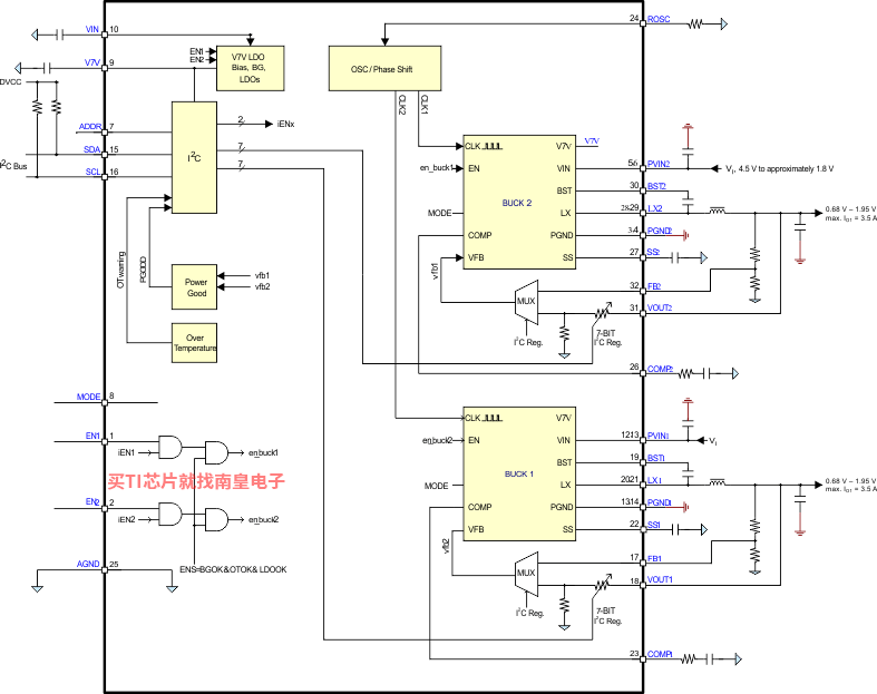
The TPS563900 device is a monolithic dual-synchronous buck converter with a wide 4.5-V to 18-V operating input-voltage range that can operate in
5-, 9-, 12-, or 15-V bus voltages and battery chemistries. Constant-frequency peak-current mode control simplifies the loop compensation and provides fast transient response.
External feedback resistors can be used to set the initial start-up voltage for each buck converter in the TPS563900 device. The feedback voltage reference for this start-up option is 0.6 V. When the voltage-identification (VID) DAC is updated through the I2C, the buck converter switches the feedback resistors from external to internal feedback resistors. The output voltage in each buck is programmable from 0.68 V to 1.95 V with 10-mV steps by I2C-controlled 7-bit VID.
Each buck converter in the TPS563900 device can also be I2C controlled for enabling and disabling the output voltage, reading the output voltage, setting the pulse skipping mode, and reading the power good status and the warning of die temperature.
The TPS563900 device features a dedicated enable pin when the I2C interface is not used. An independent soft-start pin provides flexibility in power-up programmability. Cycle-by-cycle overcurrent protection and hiccup-mode operation limit MOSFET power dissipation in short circuit or over-loading fault conditions. Low-side reverse overcurrent protection also prevents excessive sinking current from damaging the converter.
The TPS563900 device also features a light-load pulse-skipping mode (PSM) that can be controlled by the I2C or MODE pin configuration. The PSM mode allows a power loss reduction on the input power supplied to the system to achieve high efficiency at light loading.
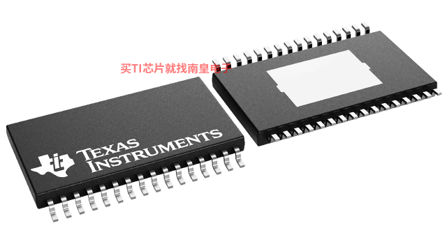
The TPS563900 device is available in a 32-lead thermally-enhanced HTSSOP (DAP) package.
- 4.5-V to 18-V Wide Input Voltage Range
- I2C Controlled 7-Bits VID Programmable Output Voltage from 0.68 V to 1.95 V with 10-mV Steps for Each Buck; Output Voltage can also be Set by Resistor Divider
- Programmable Slew-Rate Control for Output-Voltage Transition
- Up to 3.5-A Maximum Continuous Output Current in Buck 1 and Buck 2
- Buck 1 and Buck 2 can be Paralleled to Deliver up to 7-A Current
- I2C Compatible Interface With Standard Mode (100 kHz) and Fast Mode (400 kHz)
- I2C Read Back Power Good Status and Die Temperature Warning
- Pulse-Skipping Mode to Achieve High Efficiency in Light Loads
- Adjustable Switching Frequency 200 kHz to 1.6 MHz Set by External Resistor
- Dedicated Enable and Soft-Start for Each Buck
- Peak Current-Mode Control With Simple Compensation Circuit
- Cycle-by-Cycle Overcurrent Protection
- 180° Out-of-Phase Operation to Reduce Input Filter and Power Supply Conduced Noise
- Overtemperature Protection
- Available in 32-Pin Thermally Enhanced HTSSOP (DAP) Package
- Vin (Min) (V)
- 4.5
- Vin (Max) (V)
- 18
- Vout (Min) (V)
- 0.6
- Vout (Max) (V)
- 15
- Iout (Max) (A)
- 3.5
- Iq (Typ) (uA)
- 1200
- Switching frequency (Min) (kHz)
- 200
- Switching frequency (Max) (kHz)
- 1600
- Features
- Enable, Light Load Efficiency, Pre-Bias Start-Up, Synchronous Rectification, Soft Start Adjustable
- Rating
- Catalog
- Regulated outputs (#)
- 2
- Control mode
- Current Mode
- Duty cycle (Max) (%)
- 100
TPS563900的完整型号有:TPS563900DAP、TPS563900DAPR,以下是这些产品的关键参数及官网采购报价:
TPS563900DAP,工作温度:-40 to 85,封装:HTSSOP (DAP)-32,包装数量MPQ:46个,MSL 等级/回流焊峰值温度:Level-3-260C-168 HR,引脚镀层/焊球材料:NIPDAU,TI官网TPS563900DAP的批量USD价格:1.975(1000+)
TPS563900DAPR,工作温度:-40 to 85,封装:HTSSOP (DAP)-32,包装数量MPQ:2000个,MSL 等级/回流焊峰值温度:Level-3-260C-168 HR,引脚镀层/焊球材料:NIPDAU,TI官网TPS563900DAPR的批量USD价格:1.646(1000+)

TPS563900 GUI Software
PSpice for TI 可提供帮助评估模拟电路功能的设计和仿真环境。此功能齐全的设计和仿真套件使用 Cadence 的模拟分析引擎。PSpice for TI 可免费使用,包括业内超大的模型库之一,涵盖我们的模拟和电源产品系列以及精选的模拟行为模型。借助?PSpice for TI 的设计和仿真环境及其内置的模型库,您可对复杂的混合信号设计进行仿真。创建完整的终端设备设计和原型解决方案,然后再进行布局和制造,可缩短产品上市时间并降低开发成本。
在?PSpice for TI 设计和仿真工具中,您可以搜索 TI (...)


