- 制造厂商:TI
- 产品类别:电源管理
- 技术类目:直流/直流开关稳压器 - 升压稳压器
- 功能描述:适用于单节/两节电池应用的双路输出转换器(升压直流/直流 + LDO)
- 点击这里打开及下载TPS61100的技术文档资料
- TI代理渠道,提供当日发货、严格的质量标准,满足您的目标价格

The TPS6110x devices provide a complete power supply solution for products powered by either one or two Alkaline, NiCd, or NiMH battery cells. The converter generates two stable output voltages that are either adjusted by an external resistor divider or fixed internally on the chip. It stays in operation with supply voltages down to 0.8 V. The implemented boost converter is based on a fixed frequency, pulse-width-modulation (PWM) controller using a synchronous rectifier to obtain maximum efficiency.
The maximum peak current in the boost switch is limited to a value of 1800 mA.
The converter can be disabled to minimize battery drain. During shutdown, the load is completely disconnected from the battery. An auto discharge function allows discharging the output capacitors during shutdown mode. This is especially useful in microcontroller applications where the microcontroller or microprocessor should not remain active due to the stored voltage on the output capacitors. Programming the ADEN-pin disables this feature. A low-EMI mode is implemented to reduce ringing and in effect lower radiated electromagnetic energy when the converter enters the discontinuous conduction mode. A power good output at the boost stage provides additional control of cascaded power supply components.
The built-in LDO can be used for a second output voltage derived either from the boost output or directly from the battery. The output voltage of this LDO can be programmed by an external resistor divider or is fixed internally on the chip. The LDO can be enabled separately i.e., using the power good of the boost stage.
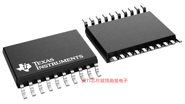
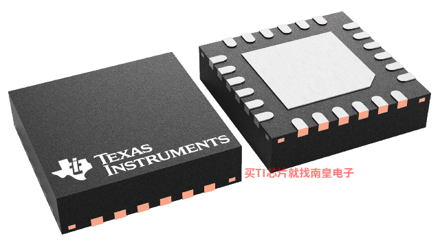
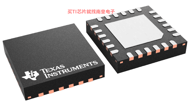
The device is packaged in a 20-pin TSSOP (20 PW) package or in a 24-pin QFN (24 RGE) package.
- Synchronous 95% Efficient Boost Converter
- Integrated 120 mA LDO for Second Output Voltage
- TSSOP-20 and QFN-24 Package
- 65 μA (Typ) Total Device Quiescent Current
- 0.8 V to 3.3 V Input Voltage Range
- Adjustable Output Voltage up to 5.5 V and Fixed Output Voltage Options
- Power-Save Mode for Improved Efficiency at Low Output Power
- Battery Supervision
- Power Good Output
- Pushbutton Function for Start-Up
- Low EMI-Converter (Integrated Antiringing Switch)
- Load Disconnect During Shutdown
- Auto Discharge Allows the Device to Discharge Output Capacitor During Shutdown
- Overtemperature Protection
- EVM Available (TPS6110XEVM-216)
- APPLICATIONS
- All Single or Dual Cell Battery Operated Products Which Use Two System Voltages Like DSP C5X Applications
- Internet Audio Player, PDAs, Digital Still Cameras and Other Portable Equipment
- Vin (Min) (V)
- 0.8
- Vin (Max) (V)
- 3.3
- Vout (Min) (V)
- 1.5
- Vout (Max) (V)
- 5.5
- Switch current limit (Typ) (A)
- 1.5
- Regulated outputs (#)
- 2
- Switching frequency (Min) (kHz)
- 320
- Switching frequency (Max) (kHz)
- 800
- Iq (Typ) (mA)
- 0.065
- Features
- Enable, Light Load Efficiency, Load Disconnect, Output Discharge, Power Good
- Duty cycle (Max) (%)
- 100
- Rating
- Catalog
TPS61100的完整型号有:TPS61100PW、TPS61100PWR、TPS61100RGER,以下是这些产品的关键参数及官网采购报价:
TPS61100PW,工作温度:-40 to 85,封装:TSSOP (PW)-20,包装数量MPQ:70个,MSL 等级/回流焊峰值温度:Level-1-260C-UNLIM,引脚镀层/焊球材料:NIPDAU,TI官网TPS61100PW的批量USD价格:2.452(1000+)
TPS61100PWR,工作温度:-40 to 85,封装:TSSOP (PW)-20,包装数量MPQ:2000个,MSL 等级/回流焊峰值温度:Level-1-260C-UNLIM,引脚镀层/焊球材料:NIPDAU,TI官网TPS61100PWR的批量USD价格:2.114(1000+)
TPS61100RGER,工作温度:-40 to 85,封装:VQFN (RGE)-24,包装数量MPQ:3000个,MSL 等级/回流焊峰值温度:Level-2-260C-1 YEAR,引脚镀层/焊球材料:NIPDAU,TI官网TPS61100RGER的批量USD价格:2.114(1000+)

PSPICE-FOR-TI ― 适用于 TI 设计和模拟工具的 PSpice
PSpice for TI 可提供帮助评估模拟电路功能的设计和仿真环境。此功能齐全的设计和仿真套件使用 Cadence 的模拟分析引擎。PSpice for TI 可免费使用,包括业内超大的模型库之一,涵盖我们的模拟和电源产品系列以及精选的模拟行为模型。借助?PSpice for TI 的设计和仿真环境及其内置的模型库,您可对复杂的混合信号设计进行仿真。创建完整的终端设备设计和原型解决方案,然后再进行布局和制造,可缩短产品上市时间并降低开发成本。
在?PSpice for TI 设计和仿真工具中,您可以搜索 TI (...)
