- ���쳧�̣�TI
- ��Ʒ�����Դ����
- ������Ŀ��LCD �� OLED ��ʾ��Դ��������
- ������������ȫ�ɱ�� LCD ƫ�� IC�����ھ��� 12 ͨ����ƽת������٤���������� GIP TV
- ������������TPS65175B�ļ����ĵ�����
- TI�����������ṩ���շ������ϸ������������������Ŀ��۸�

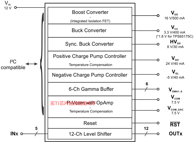
The TPS65175B/C provides a simple and economic power supply solution for a wide variety of LCD bias applications. The device provides all supply rails needed by a TFT-LCD panel but also 6 gamma references, a supply rail for LVDS support, as well as a Vcom reference. The device also integrates a VCOM_DAC rail providing the reference for an external non-inverting operational amplifier input. A 12-Channel Level Shifter is also integrated. The solution is delivered in a small 7×7 mm QFN package.
The TPS65175B/C provides a simple and economic power supply solution for a wide variety of LCD bias applications. The device provides all supply rails needed by a TFT-LCD panel. VCC and RST for the T-Con. VDD and HVDD for the Source Driver. VGH and VGL for the Gate Driver or the Level Shifters. A VCOM operational amplifier is also integrated to provide a common plane reference. The VGH and VCOM / VCOM_DAC voltages can be compensated for low and high temperatures. The transition from one programmed value to another is made using an external thermistor connected to the IC. In addition, a 6-channel Gamma Buffer as well as a 12-Channel Level Shifter are integrated. All output rails and delay times are programmable by a two-wire interface: a single BOM (Bill of Material) can cover several panel types and sizes whose desired output levels can be programmed in production and stored in a non-volatile memory embedded into the TPS65175B/C. The solution is delivered in a small 7 mm × 7 mm QFN-56 package.
- 8.6V to 14.7V Input Voltage Range
- Boost Converter VDD: 12.7V��19V (6-Bit)
- Integrated Input-to-Output Isolation Switch
- Buck Converter HVDD: VDD Tracking
- Buck Converter VCC: 1.6V...2.0V & 3.0V��3.6V (4-Bit)
- Positive Charge Pump VGH:
- 19V��34V for Low Temperature (4-Bit)
- 17V��32V for High Temperature (4-Bit)
- Negative Charge Pump VGL: �C1.8V���C8.1V (6-Bit)
- 6-Ch Gamma Buffer:
- 3-Ch: VDD��HVDD (9-Bit)
- 3-Ch: HVDD...GND (9-Bit)
- 9-Bit VCOM Reference
- 3-Bit VCOM Gain
- VCOM_DAC Output for External Operational Amplifier Reference
- Temperature Compensation for VGH and VCOM
- Reset Signal with Programmable Delay Time
- Programmable Sequencing Delays (4 �� 3-Bit)
- Thermal Shutdown
- 12-Channel Level Shifters:
- Supports Forward and Reverse Operation
- Abnormal Operation Detection
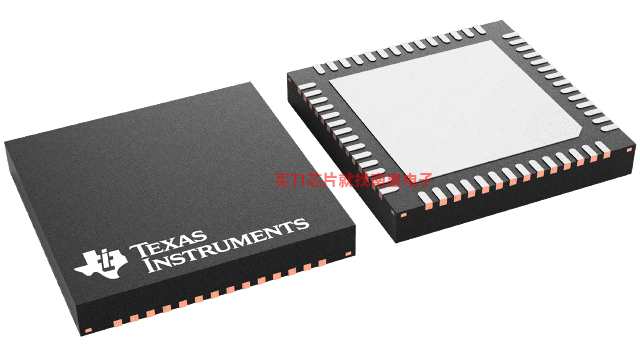
- 56-Pin 7-mm �� 7-mm QFN Package
- Display type
- LCD unipolar
- IC integration
- Gamma buffer, LCD bias, LCD level shifter, VCOM
- Vin (Min) (V)
- 8.6
- Vin (Max) (V)
- 15.5
- Source driver voltage (Min) (V)
- 12.7
- Source driver voltage (Max) (V)
- 19
- Level shifter/scan driver (ch)
- 12
- V_POS (Min) (V)
- 19
- V_POS (Max) (V)
- 34
- V_NEG (Min) (V)
- -8.1
- V_NEG (Max) (V)
- -1.8
- Features
- GPM or GVS, Gamma buffer, HAVDD, I2C interface, Level shifter, Reset generator, Temperature sensor or compensation, VCOM or op amp
- Topology
- Boost, Buck
- Rating
- Catalog
TPS65175B�������ͺ��У�TPS65175BRSHR����������Щ��Ʒ�Ĺؼ������������ɹ����ۣ�
TPS65175BRSHR�������¶ȣ�-40 to 85����װ��VQFN (RSH)-56����װ����MPQ��3000����MSL �ȼ�/��������ֵ�¶ȣ�Level-3-260C-168 HR�����ŶƲ�/������ϣ�NIPDAU��TI����TPS65175BRSHR������USD�۸�1.408��1000+��

PSPICE-FOR-TI �� ������ TI ��ƺ�ģ��ߵ� PSpice
PSpice for TI ���ṩ��������ģ���·���ܵ���ƺͷ��滷�����˹�����ȫ����ƺͷ�����ʹ�� Cadence ��ģ��������档PSpice for TI �����ʹ�ã�����ҵ�ڳ����ģ�Ϳ�֮һ���������ǵ�ģ��͵�Դ��Ʒϵ���Լ���ѡ��ģ����Ϊģ�͡�����?PSpice for TI ����ƺͷ��滷���������õ�ģ�Ϳ⣬���ɶԸ��ӵĻ���ź���ƽ��з��档�����������ն��豸��ƺ�ԭ�ͽ��������Ȼ���ٽ��в��ֺ����죬�����̲�Ʒ����ʱ�䲢���Ϳ����ɱ���
��?PSpice for TI ��ƺͷ��湤���У����������� TI (...)


