- 制造厂商:TI
- 产品类别:电源管理
- 技术类目:多通道 IC (PMIC)
- 功能描述:4.5V 至 18V 输入、3A/2A/2A 输出、三路同步降压转换器
- 点击这里打开及下载TPS65250的技术文档资料
- TI代理渠道,提供当日发货、严格的质量标准,满足您的目标价格

The TPS65250 features three synchronous wide input range high efficiency buck converters. The converters are designed to simplify its application while giving the designer the option to optimize their usage according to the target application.
The converters can operate in 5-, 9-, 12- and 15-V systems and have integrated power transistors. The output voltage can be set externally using a resistor divider to any value between 0.8 V and the input supply minus 1 V. Each converter features enable pin that allows a delayed start-up for sequencing purposes, soft start pin that allows adjustable soft-start time by choosing the soft-start capacitor, and a current limit (RLIMx) pin that enables designer to adjust current limit by selecting an external resistor and optimize the choice of inductor. The COMP pin allows optimizing transient versus dc accuracy response with a simple RC compensation.
The switching frequency of the converters can either be set with an external resistor connected to ROSC pin or can be synchronized to an external clock connected to SYNC pin if needed. The switching regulators are designed to operate from 300 kHz to 2.2 MHz. Both Bucks 2 and Buck 3 run in-phase and 180° out of phase with Buck 1 to minimize input filter requirements.
TPS65250 features a unique storage and release circuitry for dying gasp mode. The storage capacitor is separated from input capacitor during normal operation. The storage and release circuit will charge the storage capacitor with a controlled circuit to reduce the inrush current from the adaptor supply to a storage voltage of 20 V to accumulate as much energy as possible taking advantage of the 1/2 CV2 feature.
TPS65250 continuously monitors the input voltage. Once the input voltage drops below a release voltage of 10.5 V, the circuit tries to transfer charge from storage capacitor to the input capacitor keeping the input voltage closer to release value for as long as possible. The release voltage should be set lower than the processor dying gasp detect voltage. This feature greatly reduces the capacitance required to support the dying gasp operation. The storage and release circuitry is completely on chip except for the charge and storage capacitors. The control circuit makes sure that the current charging the storage capacitor is limited during power up and the storage capacitor is fully charged to its target value before the end of reset (PGOOD pin) flag to the processor is released. The circuit also features a flag signal issued to the host circuit to indicate that the ‘dump’ stage is in process (GASP pin). This signal can be used to initiate the dying gasp process and reduce the system complexity. During the release process Buck 3 must stay enabled, but Buck 1 and Buck 2 can be disabled to maximize the release time.
TPS65250 features a supervisor circuit that monitors Buck 1 and Buck 3 output voltage and generates an internal power good (PG) signal. The PGOOD pin is asserted once sequencing is done, all PG signals are reported and a selectable end of reset time lapses. The polarity of the PGOOD signal is active high.
TPS65250 also features a low power mode enabled by an external signal, which allows for a reduction on the input power supplied to the system when the host processor is in stand-by (low activity) mode.
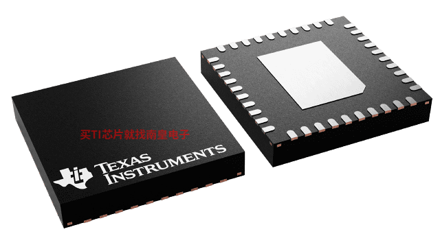
TPS65250 is packaged in a small, thermally efficient QFN RHA40 package.
- Wide Input Supply Voltage Range (4.5 V - 18 V)
- 0.8 V, 1% Accuracy Reference
- Continuous Loading: 3 A (Buck 1), 2 A (Buck 2 and 3)
- Maximum Current: 3.5 A (Buck 1), 2.5 A (Buck 2 and 3)
- Adjustable Switching Frequency 300 kHz - 2.2 MHz Set By External Resistor
- External Synchronization Pin for Oscillator
- External Enable/Sequencing and Soft Start Pins
- Adjustable Current Limit Set By External Resistor
- Soft Start Pins
- Current-Mode Control With Simple Compensation Circuit
- Power Good and Reset Generator
- Storage and Release Circuit Optimized for Reduction of Storage Capacitance in Dying Gasp Mode (Option)
- Low Power Mode Set By External Signal
- QFN Package, 40-Pin 6 mm x 6 mm RHA
- APPLICATIONS
- xDSL/xPON Modems
- Cable Modems
- Power Line Modem
- Home Gateway and Access Point Networks
- Wireless Routers
- Set Top Box
- Regulated outputs (#)
- 3
- Vin (Min) (V)
- 4.5
- Vin (Max) (V)
- 18
- Iout (Max) (A)
- 3
- Rating
- Catalog
- LDO
- 1
- Iq (Typ) (mA)
- 20
- Features
- Adjustable Current Limit, Enable, Frequency Synchronization, Power Good, Synchronous Rectification, UVLO Adjustable, Soft Start Adjustable
- Shutdown current (ISD) (Typ) (uA)
- 1300
- Configurability
- Hardware configurable, User programmable
TPS65250的完整型号有:TPS65250RHAR、TPS65250RHAT,以下是这些产品的关键参数及官网采购报价:
TPS65250RHAR,工作温度:-40 to 125,封装:VQFN (RHA)-40,包装数量MPQ:2500个,MSL 等级/回流焊峰值温度:Level-3-260C-168 HR,引脚镀层/焊球材料:NIPDAU,TI官网TPS65250RHAR的批量USD价格:1.549(1000+)
TPS65250RHAT,工作温度:-40 to 125,封装:VQFN (RHA)-40,包装数量MPQ:250个,MSL 等级/回流焊峰值温度:Level-3-260C-168 HR,引脚镀层/焊球材料:NIPDAU,TI官网TPS65250RHAT的批量USD价格:1.859(1000+)

TPS65250RHAR,工作温度:-40 to 125,封装:VQFN (RHA)-40,包装数量MPQ:2500个,MSL 等级/回流焊峰值温度:Level-3-260C-168 HR,引脚镀层/焊球材料:NIPDAU,TI官网TPS65250RHAR的批量USD价格:1.549(1000+)
TPS65250RHAT,工作温度:-40 to 125,封装:VQFN (RHA)-40,包装数量MPQ:250个,MSL 等级/回流焊峰值温度:Level-3-260C-168 HR,引脚镀层/焊球材料:NIPDAU,TI官网TPS65250RHAT的批量USD价格:1.859(1000+)