- 制造厂商:TI
- 产品类别:电源管理
- 技术类目:栅极驱动器 - 隔离式栅极驱动器
- 功能描述:具有可编程死区时间且采用 DWK 封装的汽车类 3.75kVrms、4A/6A 双通道隔离式栅极驱动器
- 点击这里打开及下载UCC21320-Q1的技术文档资料
- TI代理渠道,提供当日发货、严格的质量标准,满足您的目标价格

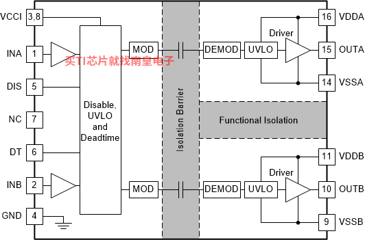
The UCC21320-Q1 is an isolated dual-channel gate drivers with 4-A source and 6-A sink peak current. It is designed to drive power MOSFETs, IGBTs, and SiC MOSFETs up to 5-MHz with best-in-class propagation delay and pulse-width distortion.
The input side is isolated from the two output drivers by a 3.75-kVRMS basic isolation barrier, with a minimum of 100-V/ns common-mode transient immunity (CMTI). Internal functional isolation between the two secondary-side drivers allows a working voltage of up to 1500 VDC.
Every driver can be configured as two low-side drivers, two high-side drivers, or a half-bridge driver with programmable dead time (DT). A disable pin shuts down both outputs simultaneously, and allows normal operation when left open or grounded. As a fail-safe measure, primary-side logic failures force both outputs low.
Each device accepts VDD supply voltages up to 25 V. A wide input VCCI range from 3 V to 18 V makes the driver suitable for interfacing with both analog and digital controllers. All supply voltage pins have under voltage lock-out (UVLO) protection.
With all these advanced features, the UCC21320-Q1 enables high efficiency, high power density, and robustness.
- 4-A peak source, 6-A peak sink output
- 3-V to 18-V input VCCI range to interface with both digital and analog controllers
- Up to 25-V VDD output drive supply
- Switching parameters:
- 19-ns typical propagation delay
- 10-ns minimum pulse width
- 5-ns maximum delay matching
- 6-ns maximum pulse-width distortion
- Common-mode transient immunity (CMTI) greater than 100 V/ns
- Universal: dual low-side, dual high-side or half-bridge driver
- Programmable overlap and dead time
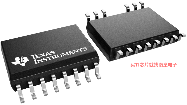
- Wide Body SOIC-14 (DWK) Package
- 3.3mm spacing between driver channels
- Operating temperature range 40 to +125°C
- Surge immunity up to 12.8 kV
- Isolation barrier life >40 years
- TTL and CMOS compatible inputs
- Rejects input pulses and noise transients shorter than 5 ns
- Fast disable for power sequencing
- Qualified for automotive applications
- AEC-Q100 qualified with the following results
- Device temperature grade 1
- Device HBM ESD classification level H2
- Device CDM ESD classification level C6
- Number of channels (#)
- 2
- Isolation rating (Vrms)
- 3750
- Power switch
- IGBT, MOSFET
- Peak output current (A)
- 6
- DIN V VDE V 0884-10 transient overvoltage rating (Vpk)
- 6250
- DIN V VDE V 0884-10 working voltage (Vpk)
- 2121
- Output VCC/VDD (Max) (V)
- 25
- Output VCC/VDD (Min) (V)
- 9.2
- Input VCC (Min) (V)
- 3
- Input VCC (Max) (V)
- 18
- Prop delay (ns)
- 19
- Operating temperature range (C)
- -40 to 125
- Undervoltage lockout (Typ)
- 12, 8
UCC21320-Q1的完整型号有:UCC21320QDWKQ1、UCC21320QDWKRQ1,以下是这些产品的关键参数及官网采购报价:
UCC21320QDWKQ1,工作温度:-40 to 125,封装:SOIC (DWK)-14,包装数量MPQ:40个,MSL 等级/回流焊峰值温度:Level-3-260C-168 HR,引脚镀层/焊球材料:NIPDAU,TI官网UCC21320QDWKQ1的批量USD价格:2.318(1000+)
UCC21320QDWKRQ1,工作温度:-40 to 125,封装:SOIC (DWK)-14,包装数量MPQ:2000个,MSL 等级/回流焊峰值温度:Level-3-260C-168 HR,引脚镀层/焊球材料:NIPDAU,TI官网UCC21320QDWKRQ1的批量USD价格:1.982(1000+)

PSPICE-FOR-TI 适用于 TI 设计和模拟工具的 PSpice
PSpice for TI 可提供帮助评估模拟电路功能的设计和仿真环境。此功能齐全的设计和仿真套件使用 Cadence 的模拟分析引擎。PSpice for TI 可免费使用,包括业内超大的模型库之一,涵盖我们的模拟和电源产品系列以及精选的模拟行为模型。借助PSpice for TI 的设计和仿真环境及其内置的模型库,您可对复杂的混合信号设计进行仿真。创建完整的终端设备设计和原型解决方案,然后再进行布局和制造,可缩短产品上市时间并降低开发成本。
在PSpice for TI 设计和仿真工具中,您可以搜索 TI (...)