- ���쳧�̣�TI
- ��Ʒ�����Դ����
- ������Ŀ��դ�������� - ����������
- �������������� 8V UVLO �� CMOS ����������� 3A��120V ����դ��������
- ������������UCC27200-Q1�ļ����ĵ�����
- TI�����������ṩ���շ������ϸ������������������Ŀ��۸�

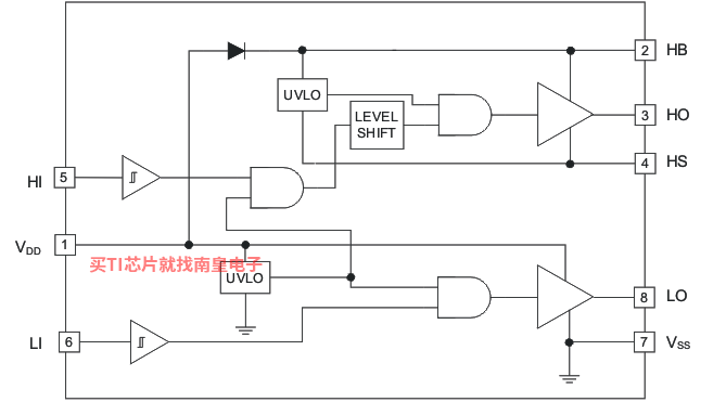
The UCC2720x-Q1 family of high-frequency N-channel MOSFET drivers include a 120-V bootstrap diode and high-side and low-side drivers with independent inputs for maximum control flexibility. This allows for N-channel MOSFET control in half-bridge, full-bridge, two-switch forward, and active-clamp forward converters. The low-side and the high-side gate drivers are independently controlled and matched to 1 ns between the turnon and turnoff of each other.
An on-chip bootstrap diode eliminates the external discrete diodes. Undervoltage lockout is provided for both the high-side and the low-side drivers, forcing the outputs low if the drive voltage is below the specified threshold.
Two versions of the UCC2720x-Q1 are offered – the UCC27200-Q1 has high-noise-immune CMOS input thresholds, and the UCC27201-Q1 has TTL-compatible thresholds.
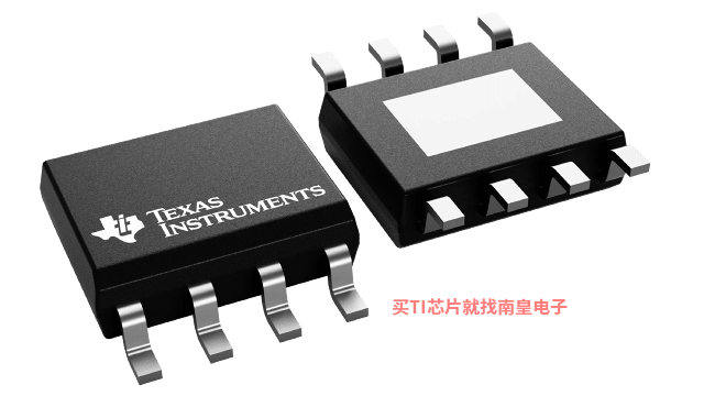
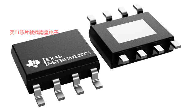
Both devices are offered in the 8-pin SO PowerPAD (DDA) package.
For all available packages, see the orderable addendum at the end of the data sheet.- Qualified for Automotive Applications
- AEC-Q100 Qualified With the Following Results:
- Device Temperature Grade 1: �C40��C to 125��C Ambient Operating Temperature Range
- Device HBM ESD Classification Level 2
- Device CDM ESD Classification Level C5
- Drives Two N-Channel MOSFETs in High-Side and Low-Side Configuration
- Maximum Boot Voltage: 120 V
- Maximum VDD Voltage: 20 V
- On-Chip 0.65-V VF, 0.6-? RD Bootstrap Diode
- Greater than 1 MHz of Operation
- 20-ns Propagation Delay Times
- 3-A Sink, 3-A Source Output Currents
- 8-ns Rise and 7-ns Fall Time With 1000-pF Load
- 1-ns Delay Matching
- Specified from �C40��C to 140��C (Junction Temperature)
All trademarks are the property of their respective owners.
- Bus voltage (Max) (V)
- 110
- Power switch
- MOSFET
- Input VCC (Min) (V)
- 8
- Input VCC (Max) (V)
- 17
- Peak output current (A)
- 3
- Rise time (ns)
- 8
- Operating temperature range (C)
- -40 to 125
- Undervoltage lockout (Typ)
- 8
- Rating
- Automotive
- Number of channels (#)
- 2
- Fall time (ns)
- 7
- Prop delay (ns)
- 20
- Iq (uA)
- 1
- Input threshold
- CMOS
- Channel input logic
- CMOS
- Negative voltage handling at HS pin (V)
- -5
- Features
- ��
- Driver configuration
- Non-Inverting
UCC27200-Q1�������ͺ��У�UCC27200QDDARQ1����������Щ��Ʒ�Ĺؼ������������ɹ����ۣ�
UCC27200QDDARQ1�������¶ȣ�-40 to 125����װ��SO PowerPAD (DDA)-8����װ����MPQ��2500����MSL �ȼ�/��������ֵ�¶ȣ�Level-2-260C-1 YEAR�����ŶƲ�/������ϣ�NIPDAUAG��TI����UCC27200QDDARQ1������USD�۸�1.156��1000+��

UCC27200 and UCC27200A PSpice Transient Model
PSpice for TI ���ṩ��������ģ���·���ܵ���ƺͷ��滷�����˹�����ȫ����ƺͷ�����ʹ�� Cadence ��ģ��������档PSpice for TI �����ʹ�ã�����ҵ�ڳ����ģ�Ϳ�֮һ���������ǵ�ģ��͵�Դ��Ʒϵ���Լ���ѡ��ģ����Ϊģ�͡�����?PSpice for TI ����ƺͷ��滷���������õ�ģ�Ϳ⣬���ɶԸ��ӵĻ���ź���ƽ��з��档�����������ն��豸��ƺ�ԭ�ͽ��������Ȼ���ٽ��в��ֺ����죬�����̲�Ʒ����ʱ�䲢���Ϳ����ɱ���
��?PSpice for TI ��ƺͷ��湤���У����������� TI (...)
