- 制造厂商:TI
- 产品类别:电源管理
- 技术类目:栅极驱动器 - 低侧驱动器
- 功能描述:具有反相/非反相输入的汽车类 4-A/4-A 双通道栅极驱动器
- 点击这里打开及下载UCC27425-Q1的技术文档资料
- TI代理渠道,提供当日发货、严格的质量标准,满足您的目标价格

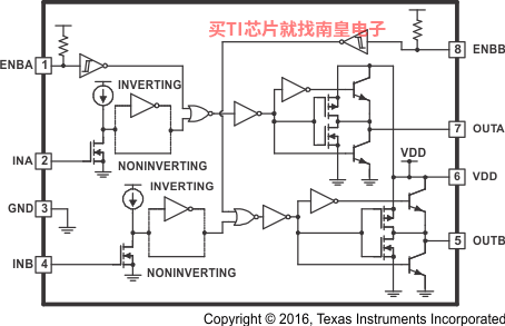
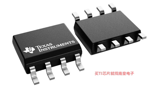
The UCC2742x-Q1 family of devices are high-speed dual MOSFET drivers capable of delivering large peak currents into capacitive loads. Two standard logic options are offered: dual inverting and dual noninverting drivers. They are offered in the standard 8-pin SOIC (D) package. The thermally enhanced 8-pin PowerPAD Package MSOP package (DGN) drastically lowers the thermal resistance to improve long-term reliability.
Using a design that inherently minimizes shoot-through current, these drivers deliver 4-A current where it is needed most, at the Miller plateau region, during the MOSFET switching transition. A unique bipolar and MOSFET hybrid output stage in parallel also allows efficient current sourcing and sinking at low supply voltages.
The UCC2742x-Q1 provide enable (ENBL) functions to have better control of the operation of the driver applications. ENBA and ENBB are implemented on pins 1 and 8, which were previously left unused in the industry standard pinout. They are internally pulled up to VDD for active-high logic and can be left open for standard operation.
For all available packages, see the orderable addendum at the end of the data sheet.- Qualified for Automotive Applications
- AEC-Q100 Qualified With the Following Results:
- Device Temperature Grade 1: –40°C to +125°C Ambient Operating Temperature Range
- Device HBM ESD Classification Level 2
- Device CDM ESD Classification Level C6
- Industry-Standard Pinout
- Enable Functions for Each Driver
- High-Current Drive Capability of ±4 A
- Unique Bipolar and CMOS True Drive Output Stage Provides High Current at MOSFET Miller Thresholds
- Inputs Independent of Supply Voltage Compatible With TTL and CMOS
- 20-ns Typical Rise and 15-ns Typical Fall Times With 1.8-nF Load
- Typical Propagation Delay Times of 25ns With Input Falling and 35ns With Input Rising
- 4-V to 15-V Supply Voltage
- Dual Outputs Can Be Paralleled for Higher Drive Current
- Available in Thermally Enhanced MSOP PowerPAD Package
- Rated From –40°C to +125°C
All trademarks are the property of their respective owners.
- Number of channels (#)
- 2
- Power switch
- MOSFET, IGBT
- Peak output current (A)
- 4
- Input VCC (Min) (V)
- 4
- Input VCC (Max) (V)
- 15
- Features
- Enable Pin
- Operating temperature range (C)
- -40 to 125
- Rise time (ns)
- 20
- Fall time (ns)
- 15
- Prop delay (ns)
- 25
- Input threshold
- CMOS, TTL
- Channel input logic
- Inverting, Non-Inverting
- Input negative voltage (V)
- 0
- Rating
- Automotive
- Driver configuration
- Inverting, Non-Inverting
UCC27425-Q1的完整型号有:UCC27425QDRQ1,以下是这些产品的关键参数及官网采购报价:
UCC27425QDRQ1,工作温度:-40 to 125,封装:SOIC (D)-8,包装数量MPQ:2500个,MSL 等级/回流焊峰值温度:Level-1-260C-UNLIM,引脚镀层/焊球材料:NIPDAU,TI官网UCC27425QDRQ1的批量USD价格:.519(1000+)

UCC27425 PSpice Transient Model
PSpice for TI 可提供帮助评估模拟电路功能的设计和仿真环境。此功能齐全的设计和仿真套件使用 Cadence 的模拟分析引擎。PSpice for TI 可免费使用,包括业内超大的模型库之一,涵盖我们的模拟和电源产品系列以及精选的模拟行为模型。借助?PSpice for TI 的设计和仿真环境及其内置的模型库,您可对复杂的混合信号设计进行仿真。创建完整的终端设备设计和原型解决方案,然后再进行布局和制造,可缩短产品上市时间并降低开发成本。
在?PSpice for TI 设计和仿真工具中,您可以搜索 TI (...)


